Actually manufacturing costs are pretty low, you can get pretty good quality PCBs from Chinese fab houses quite cheaply. Assembling is the expensive service.
Precisely that.
Actually manufacturing costs are pretty low, you can get pretty good quality PCBs from Chinese fab houses quite cheaply. Assembling is the expensive service.
Precisely that.
Well that’s good to know about both those things. If I come up with extras, then I’ll give them away at a meetup or something.
Would you then describe my idea as fairly straightforward? I suppose I’m trying to gauge the mindset at which I should approach my project.
Also, is FR4 material relatively inexpensive? I figured I would just do a FR4 sandwich case while I’m at it.
FR4 is an specification for fiberglass and epoxy resin panel. As a matter of fact, FR stands for Flame Retardant. It is pretty cheap and I’ve already seen people using it as case material before, even outside the mechanical keyboards community.
Yeah, FR4 sandwich cases are pretty good, I actually like them better than acrylic due to the increased stiffness of the material even with thin layers. It’s even rather simple to get a case made, just use KLE and SwillKB to make a plate design, export it in dxf, then you can import it into KiCad to use as an edge cuts layer. Also, I recommend JLCPCB for their quick turnaround and good prices.
That’s even better to hear! I’ve used those well enough. Would anyone here be willing to review my design as I struggle with it?
The only issue with that though is when you no longer are a student, it’s expensive. So taking the time to learn Kicad now which is free and has a lot of features, means you’ll have access and ability to use it well after you graduate.
I’m the one who designed the Catch22 kit (PCB, plate, etc.). I’d be happy to help you with whatever you need! PCB design offers a whole new level of creativity and customization.
The one thing to keep in mind is that you can’t sell things that you make with a student license. Don’t know how strict Autodesk is, but it is technically against the license policy to commercialize Eagle designs without paying for a professional license.
If anyone’s interested, I have a basic Cherry MX library for Eagle. Not battle-tested tough…
EDIT: seeing there’s a new library for Eagle that I had no idea about few months back, feel free to ignore me 
I made my own MX library years ago, it’s available on my Github. And those are battle-tested, my custom boards and the Sentraq S60-X were designed using it. ![]()
Man, another resource…twice in two minutes 
Starred, I guess I’ll give it a shot.
I’m at the point of moving the footprints around. Is the best way to ensure that the footprints are in the right place by importing that DXF to something like an Eco or Comments layer?
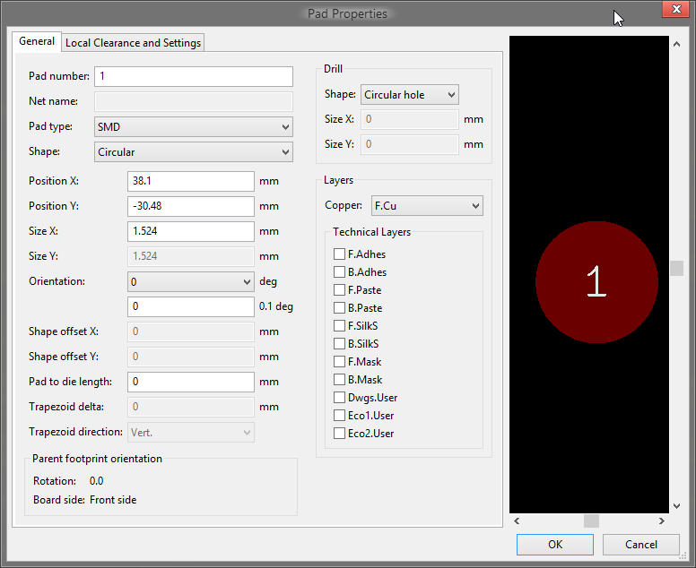
You’re going to want a separate project file for each plate since they’ll each be their own PCB. In each of these project files you’ll create a new footprint that contains the plate DXF imported to the Edge Cuts layer and an SMD pad on either side only in the copper layer for each side.

SMD Pad 1 on F.Cu, Pad 2 is the same but on B.Cu.
What this does is make the plate look like a component electrically and help keep from confusing PCB fabs when they’re checking it over.
Next, you’ll want to make a super simple schematic with a single resistor hooked to ground on both sides, then associate it with your footprint you just made when you export the netlist.
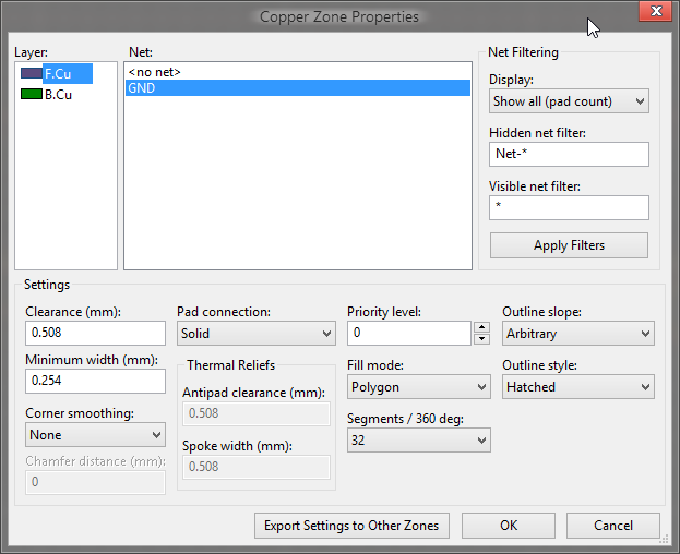
Finally, you’ll want to open the PCB file for this project and read the netlist, which will place your plate file. You then add a copper zone on both sides that are part of the ground net.

Both zones are part of the GND net.
You could just import the DXF to the PCB file and throw planes onto either side, but this may cause issues with some PCB fabs when they check over the design since they’re expecting it to play nicely electrically.
You can now add silkscreen designs to your liking and then you’ll plot your gerbers with front and back copper, silk, mask, and edge cuts layers.
Hopefully this is simple enough to follow along but let me know if it isn’t. With this method there’s really nothing to line up, the entire PCB plate will be just that footprint you make and you’ll need 1 PCB per plate you make.
Wow. This is great. Its EXACTLY what I needed.
Another noob question:
Can I connect a trace to the middle of another trace?
For example, if I’m thinking of a hand-wired board and I wired any given column, let’s say, I can choose to wire that column to the controller at really any point on the column.
For a PCB, can I treat the traces the same, where I can tie into the middle of a trace? Or do I need to daisy chain the relevant pads together and then connect to the controller?
Man, I hope that made sense…
You can, but it isn’t considered a best practice. Realistically speaking this only really matters when dealing with radio frequencies (RF), which isn’t the case with keyboards.
Unless you are trying to design a Bluetooth-connected keyboard, then it matters a lot. 
Does anyone have or know of any orcad libraries? I use orcad for schematics at work and picked up a discounted license recently, but all my layout experience is with altium and I basically have nothing to start with for personal projects with orcad. I have no problem doing it myself but if there is anything out there it would be a nice kick start for my project.
The last time I had contact with Orcad was in the mid to late 90s, a pirated copy of a DOS version. Never liked it very much, to be honest.
It’s not a very good tool tbh, but sadly it’s the industry standard. Three of the last four places I’ve worked have used it (the fourth used altium). I figure if it’s what I use in a professional environment I might as well use it at home too. The support is pretty good and it’s usually not too hard to find symbols/footprints since so many people use it.