The Phoenix Project No 1, a PCB replacement for the RAMA M65-A keyboard (now open source !)

Hello keeb lovers,

It looks to be of interest to several people in this hobby to revive their older custom boards, often staying in their box or taking dust because of no more working of unstable PCBs.

And it looks to be true for the very beautiful M65-A keyboard made by RAMA, plagued with PCB issues, see in the link below:
M65-A Replacement PCB

So I decided to do something to remediate that and ‘The Phoenix Project’ was born.
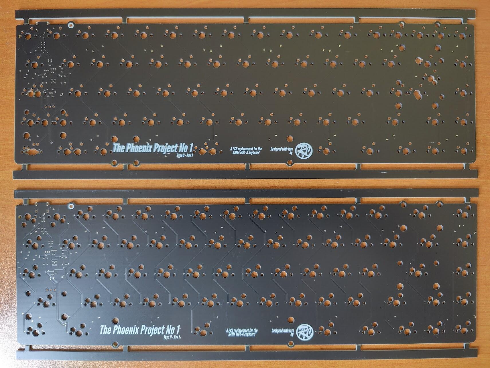
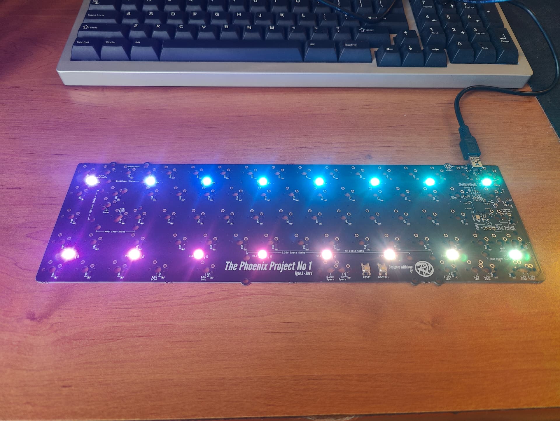
We are talking about the M65-A replacement PCB, and it the first (No 1) of maybe future efforts to make those old nice customs clack again.

As it was not clear if a hotswap or solder PCB would be preferred I have designed both:

  • Hot swap: The Phoenix Project No 1 - Type H
  • Solder: The Phoenix Project No 1 - Type S

Those two versions have a lot in common:

  • Both are electrically compatible and should share the same QMK/VIA/VIAL firmware.
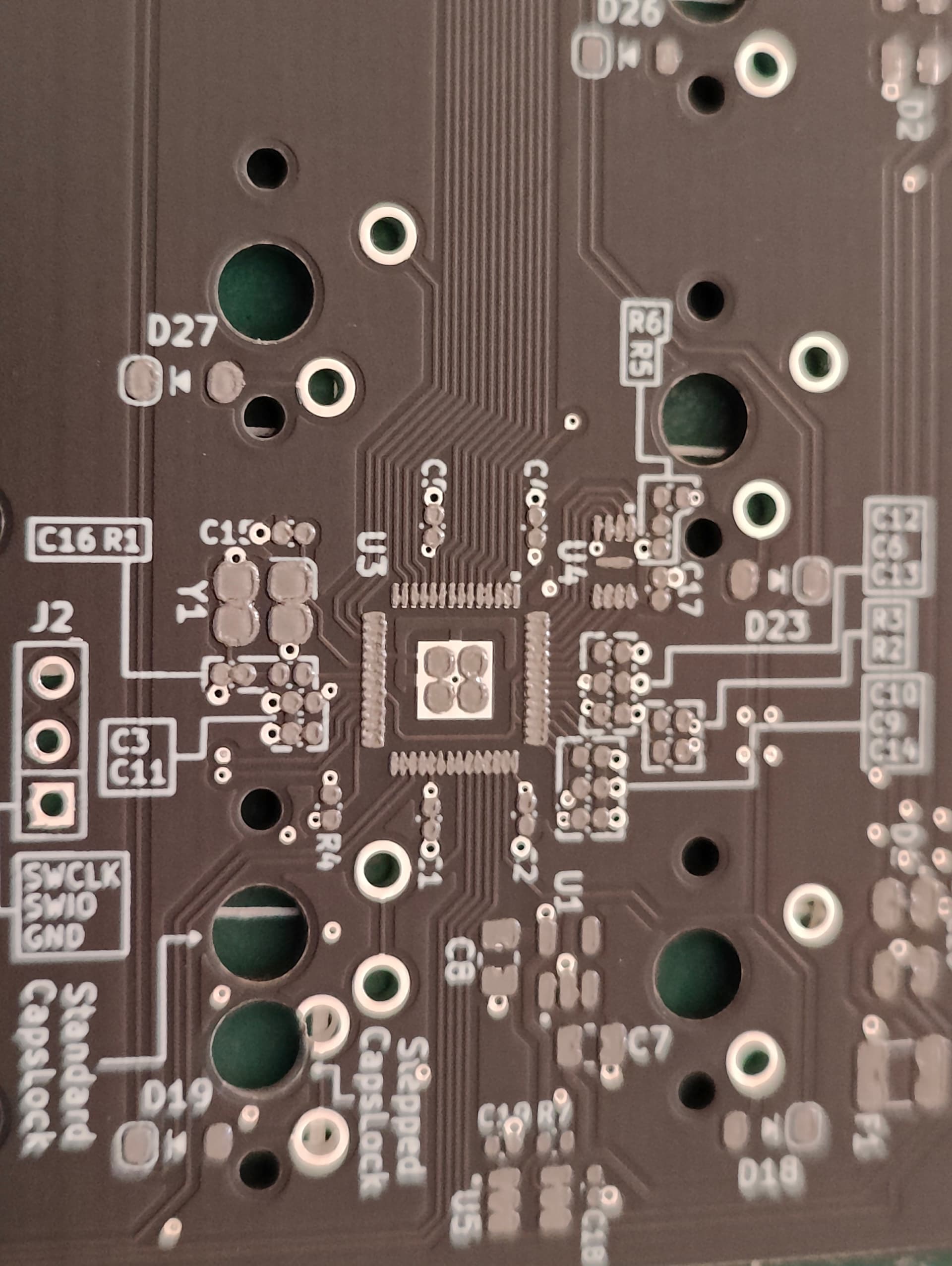
  • RP2040 MCU with 2MB flash memory.
  • Underglow RGB.
  • ESD protection for USB VBUS and data lines.
  • EMI protection with a ferrite bead.
  • Overcurrent protection with a resettable fuse.
  • No key lighting (uniform lighting is present on the original PCB).
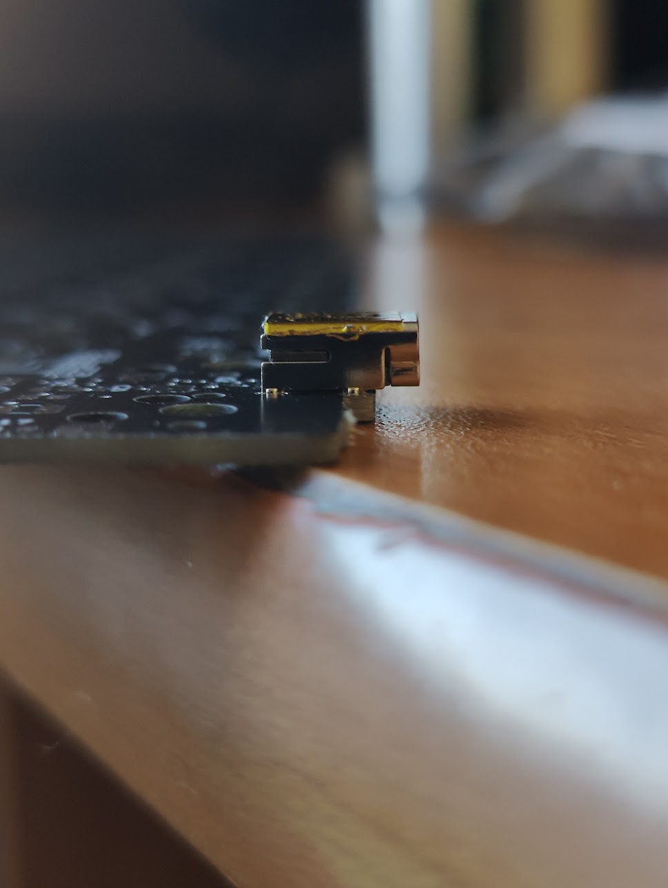
  • Good old USB mini connector like on the original PCB.
  • Reset and Bootsel buttons.
  • Header for SWD debugging.

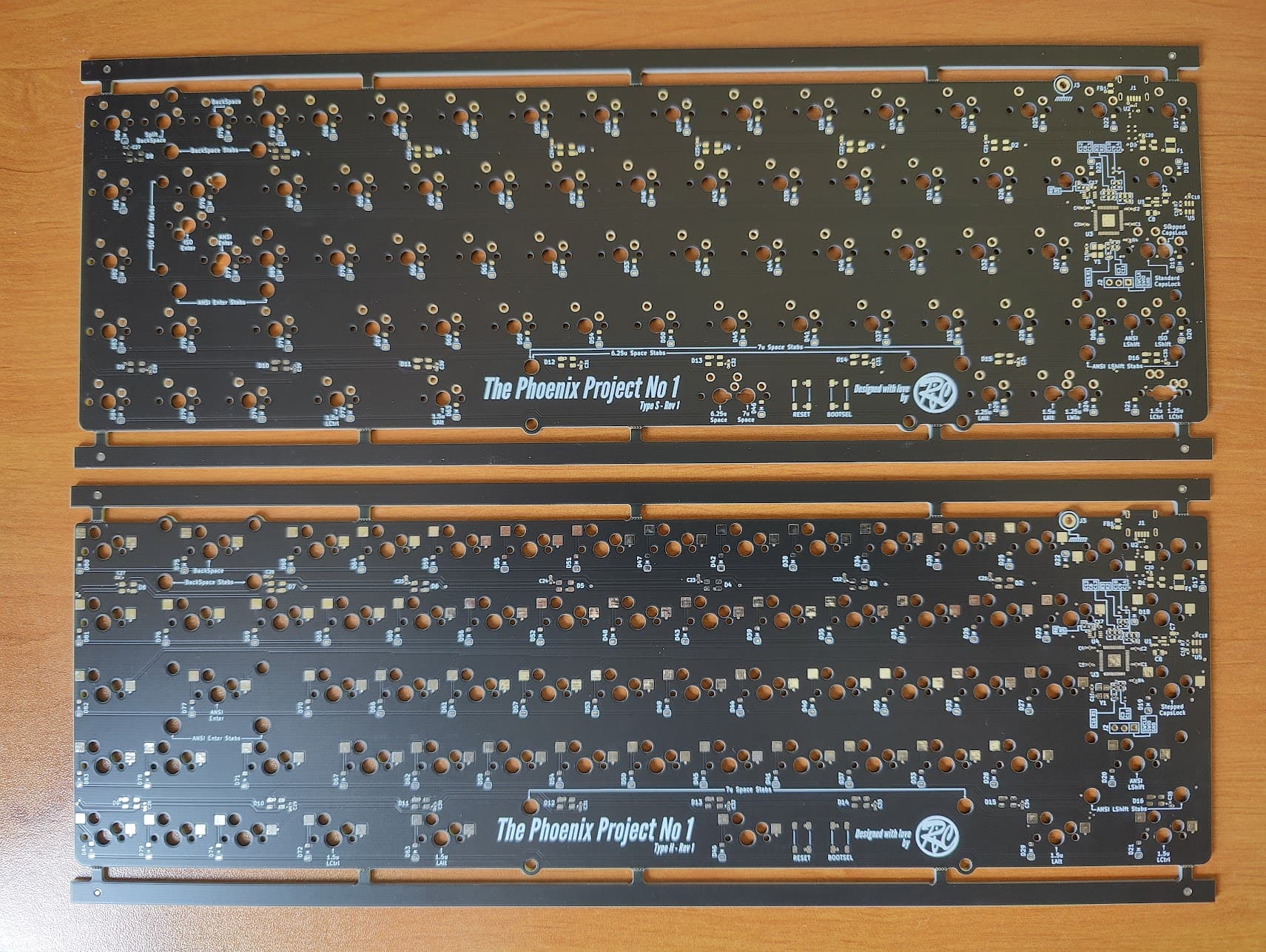
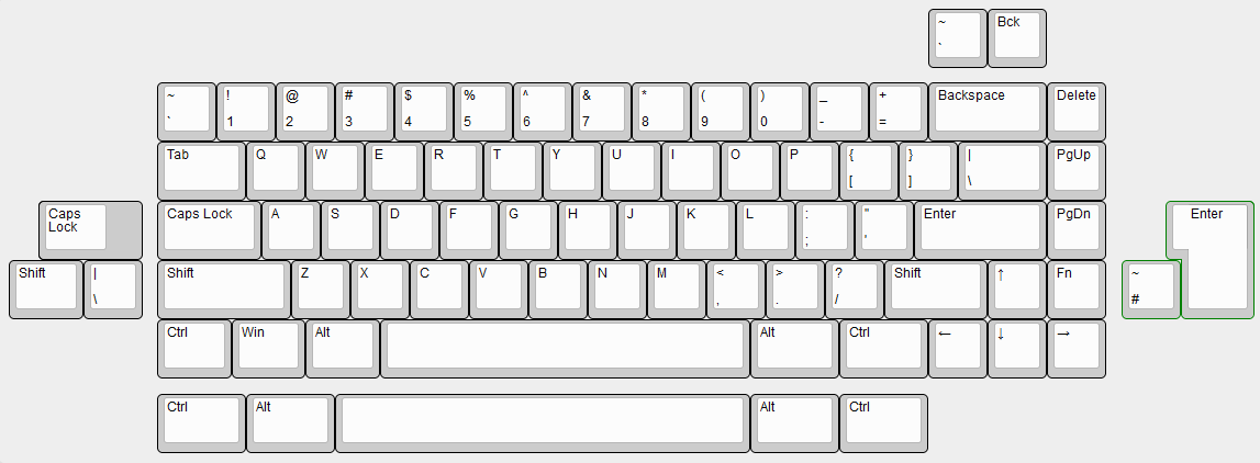
As for the selected layouts, only one is available for the Type H:

  • Full backspace
  • Stepped Caps Lock
  • Winkeyless Tsangan bottom row (7u spacebar and 1.5u mods)

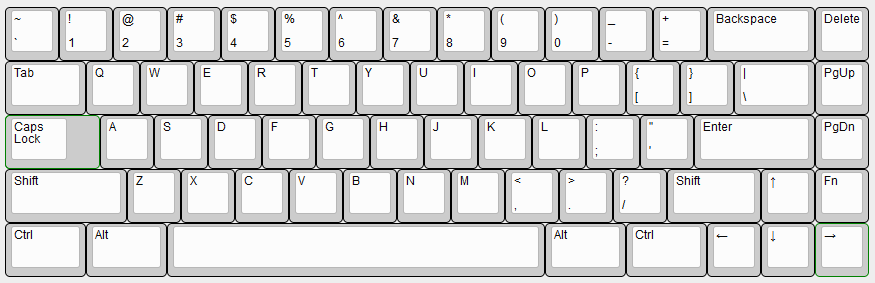
A you see this is not a normie layout like you can usually have on a hotswap board, this layout may potentially please to people that often look at a solder PCB to have this kind of layout.

The Type S has a more extensive layout, including ISO, without going crazing in order not to have a PCB Swiss Cheese.

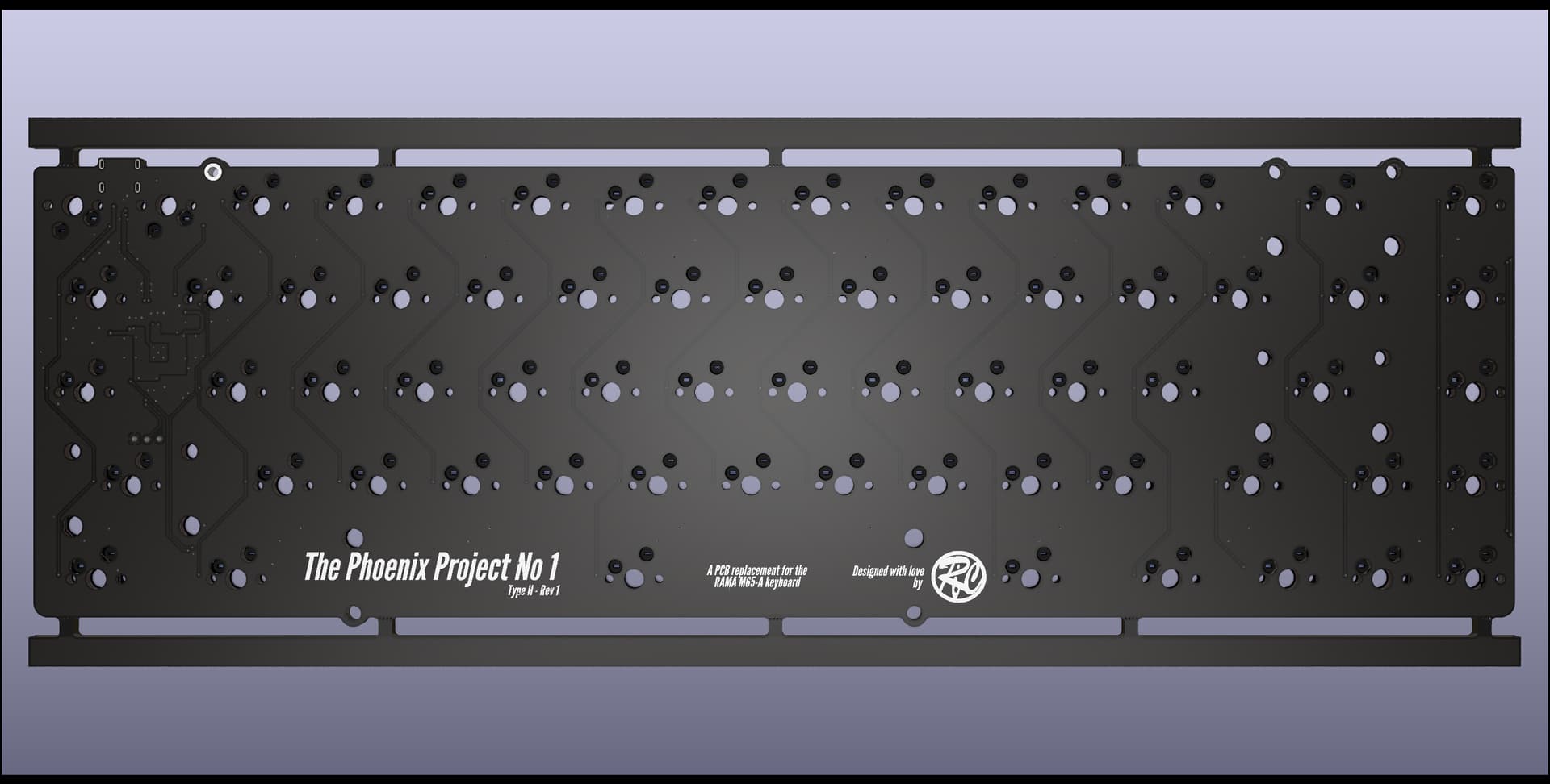
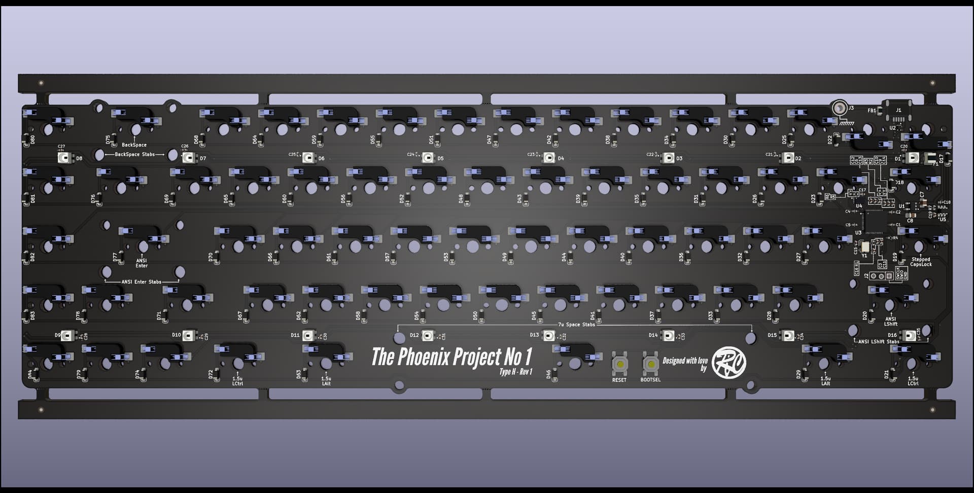
Here are some Kicad renders for the Type H:
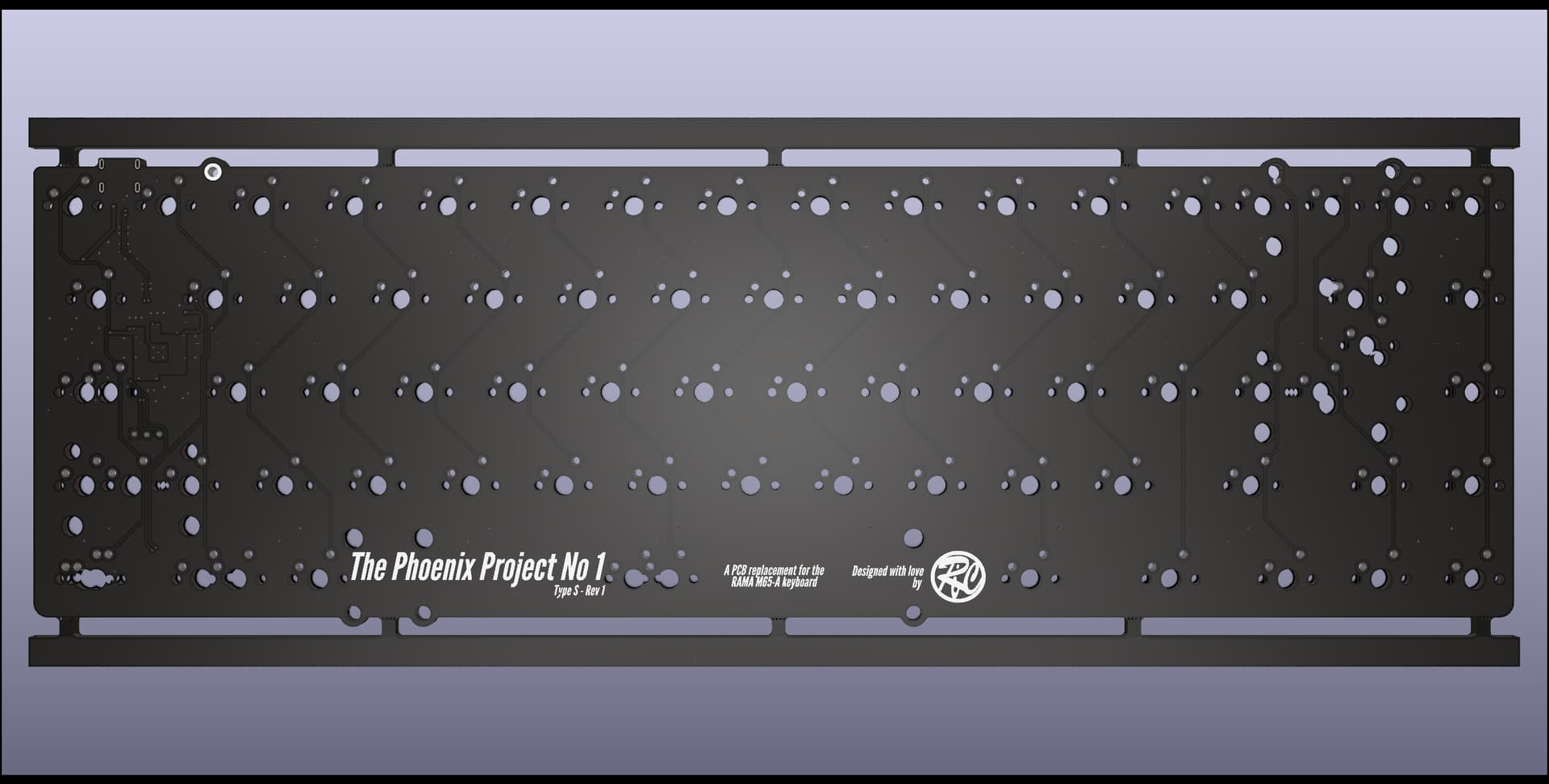

And for the Type S:


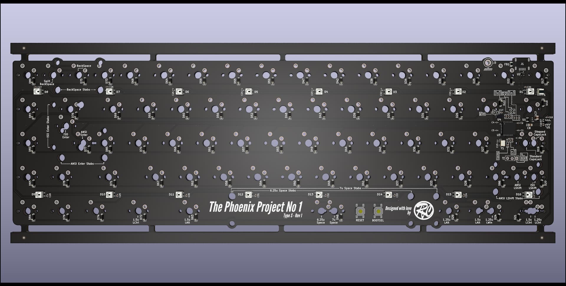
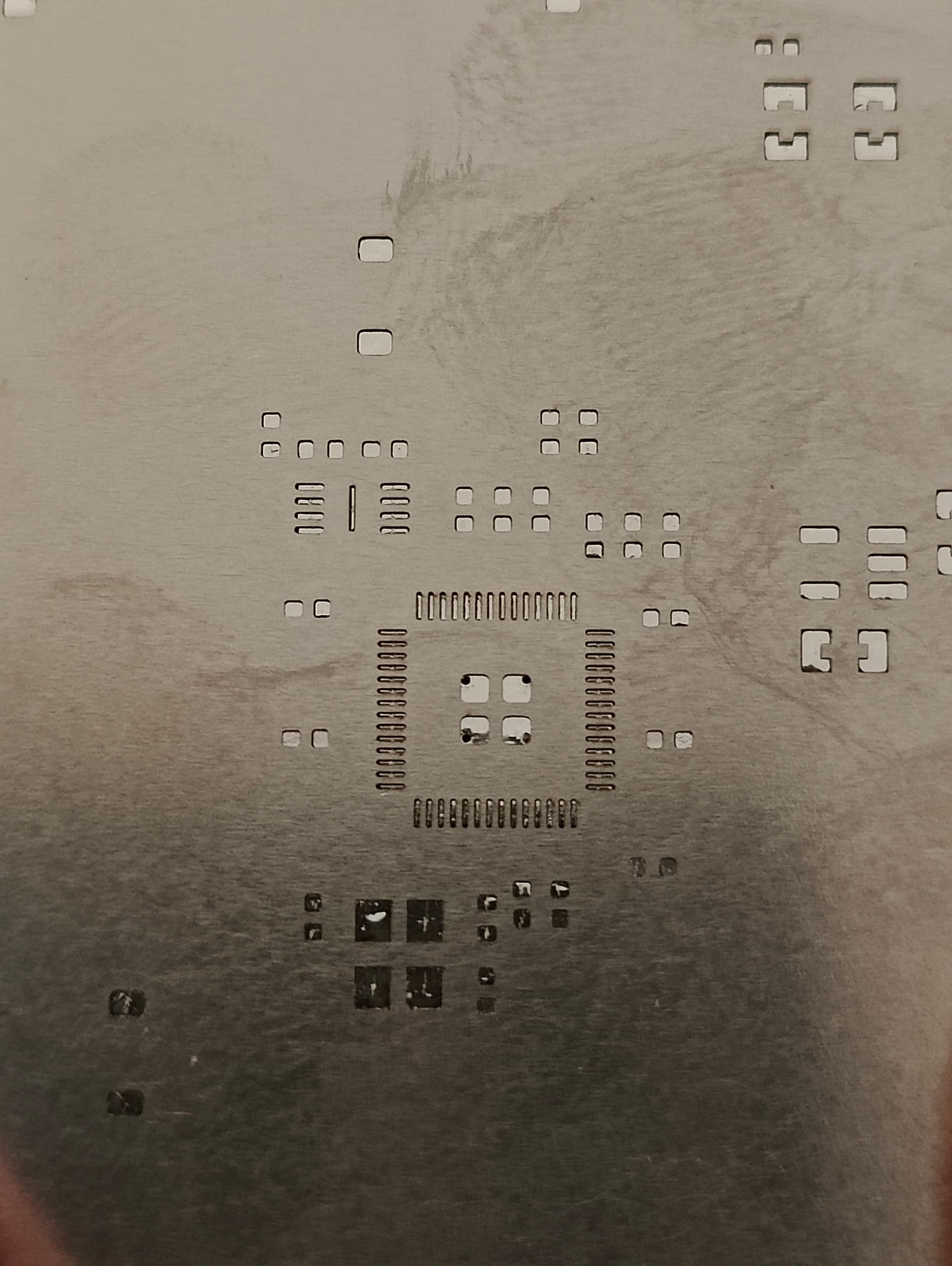
Did you see the protruding hole near the USB port ?
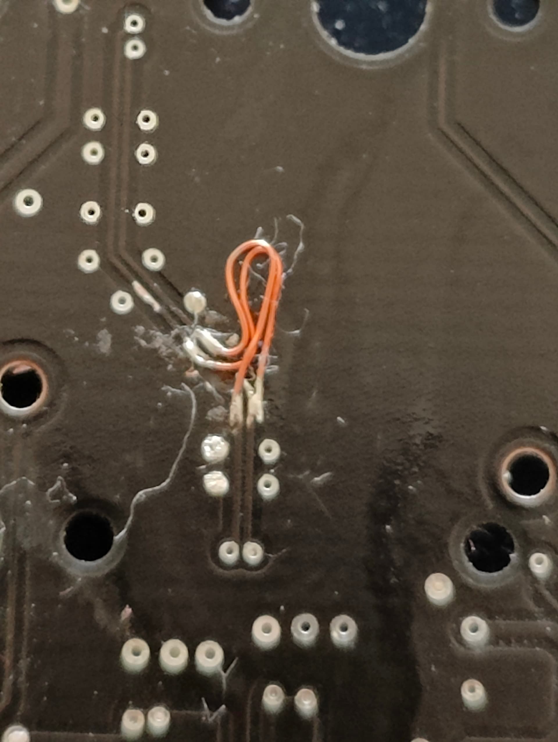
This is to solder a wire attached to a connector that will be later screwed to the case.


I did that because specially on Nylon bottom versions of the board a lot of static can be generated and this could ESD zap several components on the PCB. This will allow to have the case properly grounded and hopefully make the PCB much more ESD safe.

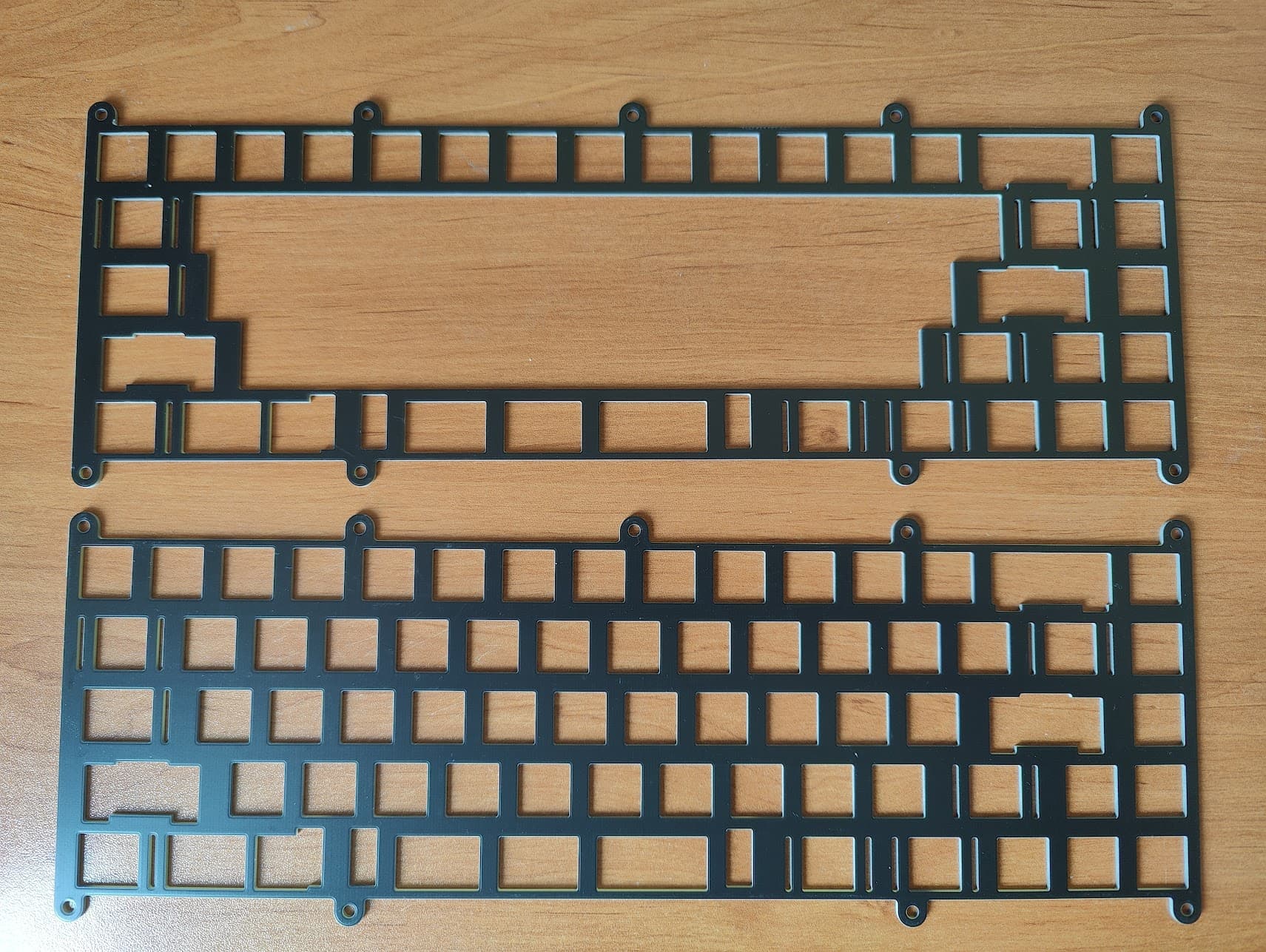
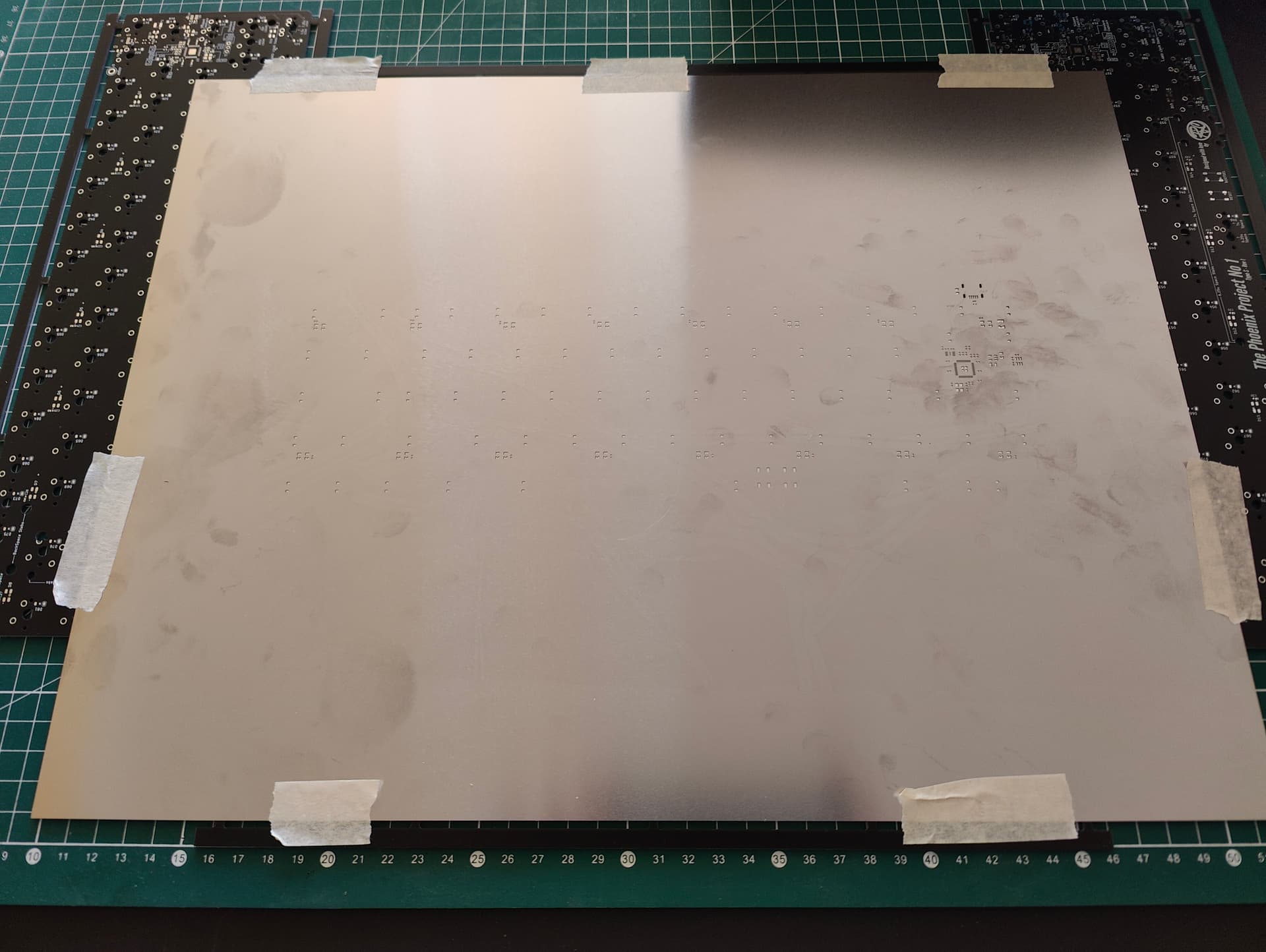
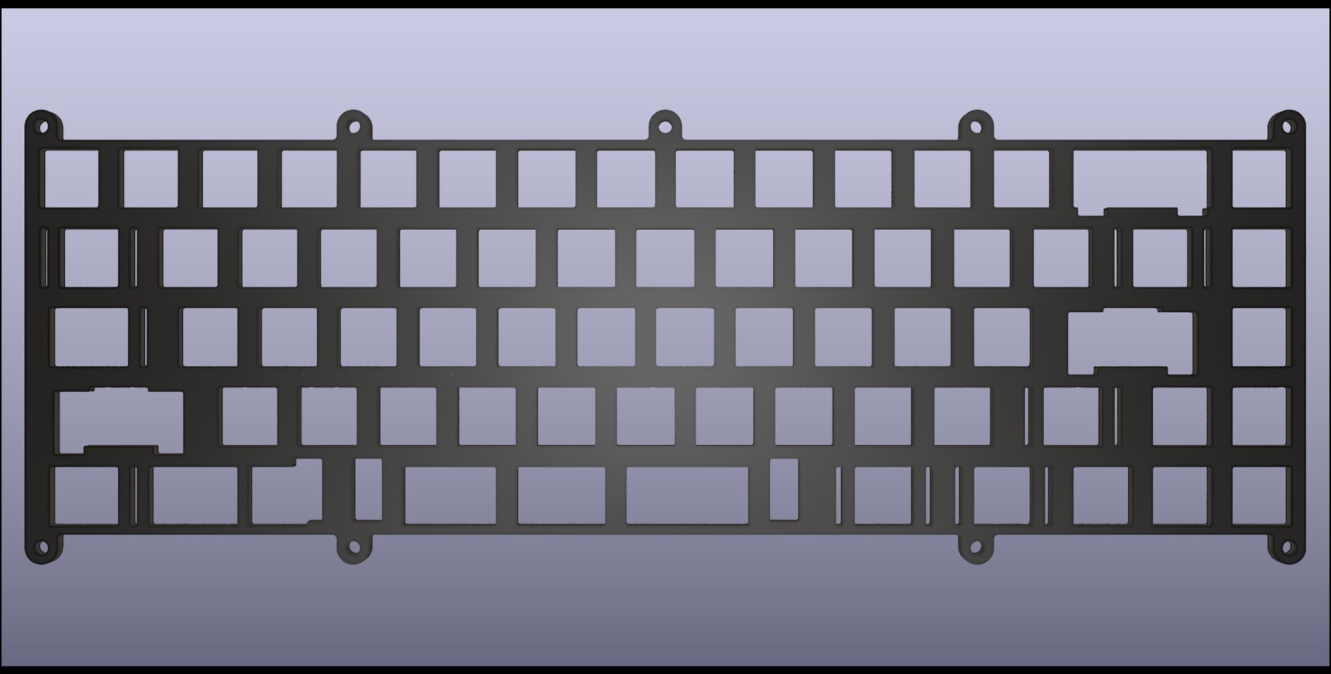
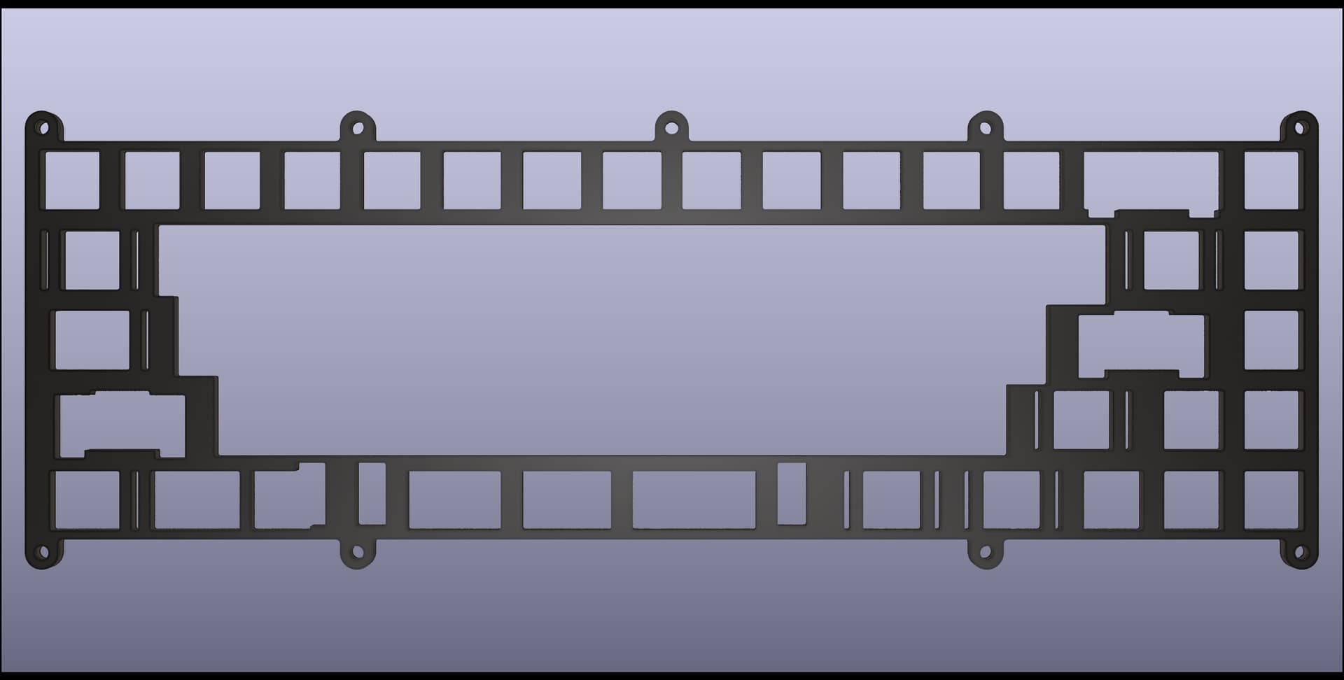
Also designed several plate options, half plate and full plate, but you could still use the plate that came with your board.
If you look carefully not all screw holes are used on those plates, and specially under the space bar.
This is done in the hope to have a bit less stiff typing experience compared to the original plates.
Also there are cutouts under the spacebar in order to thin out the sound of this key a bit.
Most obvious formats will be .DXF and .STEP so that anyone could make their own in the future.
Also have a PCB version of the plates as you can see below in the Kicad renders.


The status of the project is not yet complete, but already ordered 5 units of each PCB and plate versions, all with black solder mask.
Need to assemble them by hand before conducting tests to check that I’ve done everything well.

When the project will be in a shape that I think is good enough, I will open source it with a permissive licence so that anyone will be able to manufacture it without asking anything, even vendors.
Time has been taken so that even individuals can order their own assembled PCBs at JLCPCB, all components used are available on their website, the only thing is some components can be out of stock sometimes (this is the case now for the RP2040 MCU and the Kailh hot swap sockets).

I’d like to thank our good buddy @pixelpusher for all the great information and feedback he gave me during the designing process, thank you so much dude !

10 Likes

Excited to finally see the bird rising from its ashes!

2 Likes

Awesome! Thank you for all your arduous work on this.

I will be grabbing a couple for sure :grin:

1 Like

If the design proves to work as intended why not :wink:
This will help me mitigate the cost prototyping, haha !

I will have around 5 hotswap PCBs, 5 solder PCBs, 5 full plates and 5 half plates.
A few of them will be kept for testing, but there will definitively be a few left !

1 Like

I’m not on this forum much and I would be in for a spare or two. Hopefully I will be aware when this goes live but if you can cross post to the original groupbuy on GH like pixel did, I’m sure I’ll jump in.

Thanks for doing this, and yeah as you mentioned I’ve bought spare PCBs for some classics and will continue to do so, good luck and please don’t give up!

2 Likes

Will share on GH for any news may have!

1 Like

Just received the PCBs (not assembled) from JLCPCB!

And also have the plates :wink:

Waiting for the components now …

5 Likes

:raised_hands: :heart_eyes::star_struck::partying_face:

Curious how are you planning to assemble. I like to watch people stencil and bake, but drag soldering and hot air stations with lots of flux involved are fun as well

1 Like

I also ordered stencils :wink:

Will do full hot air soldering this time !

1 Like

I don’t think you understand how happy finding this thread has made me. I have had a m65a with a PCB I butchered when desoldering like 2.5 years ago right at the start of covid. I finally got a dz65 pcb and was going to either jam it in or just dremel out the USB hole. This has entirely changed the game for me! Can’t wait to see how this goes and would love get my hands on one of these.

2 Likes

After a long wait, and being afraid that the package would be lost, I finally received the components to solder the PCBs !

Wanted to immediately test fit the mini USB connector.
Selecting the correct USB connector gave me a little bit of trouble as the previous reference I used was not sticking out enough from the PCB (only 1.2 mm).
Thanks to @pixelpusher that made measurements on it’s own PCB, I knew that I had to roughtly have a stick out of about 2.5mm to 3mm to be in the same leage as the original PCB.
Quite a significant time have passed looking at a miriad of references, each looking at the datasheet to find the correct stick out.
Found a reference that was fitting the needs and I made a custom Kicad footprint for it.
Was a bit afraid of doing something wrong, a mistake can easily happen who would render the PCB useless.

It fits perfectly, and it looks to stick out from the PCB of the correct amount (about 2.6mm using calipers).
Yay!

2 Likes

Didn’ t gave any news since I received the PCBs and components.
The reason is, making the first PCB work has been a rocky experience …
Let’s explain a bit in details below.

One week ago I soldered the first (and only) PCB, selected the soldered version as I didn’t want to waste any hotswap socket in case something goes wrong.

First step is to place the stencil and secure it onto the PCB.
The stencil size is quite huge, had to rely on using four other PCBs to properly fix it.

Aligning pads is a rather tedious process, the size of the stencil does not help but also the small 402 smd components adds to the challenge and forces me to use magnifying glasses.
Here is a zoom of the result after correct alignment.

Time to dispense my favorite low temp solder paste.

The paste is correctly dispensed but something looks odd: the paste looks significantly dryer than usual.
And this will generate the problem that I had to solve.

  1. Problem 1

After reflow using my hot air soldering station, the pads looked like they were not correctly reflowed and I had a lot of solder balls everywere.
I had to rely on retouch every pads with my soldering iron to cleran them out, a lengthy process.
Time to buy new solder paste !
This has been the first of many problems to come…

  1. Problem 2

By plugging the PCB nothing happened but the resettable fuse was getting super hot, showing that I had a USB 5v short somewhere (and I should have tested that with a multimeter before plugging the board).
Time to figuring out who causes the problem, and this can be anything from the USB connector to the voltage regulator on the 5V side and any bypass capacitor on the 5V domain.
After desoldering many components, found that one of the LEDs bypass capacitors was the culprit.
No more shorts now but this took me a lot of time…

  1. Problem 3

Those are a result of the too old paste and my imperfect attempt to reflow the pads:

  • No 3V3 current were going the MCU, dry solder pad problem.
  • One of the crystal pads were shorted.
  1. Problem 4

Still not booting to the bootloader …
And the last problem was in the PCB design: I inverted the USB D+ and D- lines :frowning:
Had to cut those traces and reroute them with enamel wire.

This is of course ugly but it does not prevent the switches to be installed.
And after a bit of electrical tape it is a bit more acceptable.

After all that effort the PCB goes to the bootloader nicely :slight_smile:
Also the LEDs blinked briefly during that time, proving that they are working.

Conclusion:

Still have to write a firmware on it to check any other potential problems, but it looks like it wants to work :wink:
The PCB should probably be usable without any trouble and could be used for testing on a board, but is not pretty to look at due to the great amount of rework.
Already started doing modifications on my design in order to have all problems fixed.

See you later !

2 Likes

Was just thinking about this last night. Looks like you’re getting down into the weeds and making your way back out! Fun! I’ve been watching a lot of YouTube videos of electronics repairs and I love it.

1 Like

I’m assuming you’re doing the assembly yourself for the fun of it, but what is the price difference between what you ordered and getting it filly assembled at the factory?

1 Like

Yes, it is very similar to try to repair an existing electronic product.

This process of figuring out what was wrong and fixing it was retrospectively fun, I learned a lot in the process !

Part of it is for fun and try to improve on solering skill.

As it involves my own money another factor is cost for such a small number of units.
Also I had the feeling already that I’d make minor mistakes here and there and that the final ‘clean’ PCB would need another revision; so it happened that it was the right decision :wink:

The total cost for 5 solder PCBs, 5 hotswap PCBs, 5 full plates and 5 half plate have been around 400€ if I remember (including taxes and shipping if I recall). That would mean at cost it is around 40€ for both a PCB and a plate.

Let’s say that a soldered PCB is usually sold at 45-50€ and a hot swap version at 55-65€.
If I were to sell those at cost and use JLCPCB assembly service, I think that a good starting number of units would be around 10.
Other PCB manufacturing companies like PCBWay are significantly more expensive for low number of units, but as the number of units grows the price begins to be more and more interesting.

So I’d say JLCPCB for low volume production (interesting up to 50 units?), and other PCB manufacturers for higher volumes.

For Revision 2 of the PCBs I plan to try to make them fully assembled, at least 2 units of each type.
This would validate the process for any user to order at JLCPCB and have everything assembled.

2 Likes

Some quick news.

Had the time to write the QMK/VIAL firmware for the PCB and it works perfectly !!!

Worked first time, all RGB underglow effects work nicely, and also all keys and layout combinations :slight_smile:

This is a perfectly working PCB that could be used for fit testing on a real M65-A keyboard!

2 Likes

Hey! I jumped on the M65-a train the moment I saw the first render and I’m currently on my third jc65 PCB. The first two had the LEDs break after a few months, and after using the board for a year without backlighting it stopped working on my mac, and then finally died altogether shortly after. I put it in storage for a few years before I got it out again two months ago. After I resoldered it again it started acting up after a few weeks and… I don’t know, I just wanted to say that finding this thread made me so happy.

I hope you’ll be able to sell these soon! Wishing you the best!

2 Likes

Hello,

I may have a few PCBs soldered when revision 2 will be done.
I do not plan to make a business of it, but it should be possible to sell a few at cost to people in need like you .
The master plan is to make the design open source so that any vendor could manufacture and sell them in the future, and also individuals.

1 Like

Of course, I gathered that much from skimming through the two threads. I just wanted to chime in and show my support and appreciation for the amazing work you’re doing. This really is important, seeing all of these boards bricked breaks my heart (and I’m a champion of reuse and buying things for life so minimizing waste is dear to me). If you’re in a position to send off a demo board I’d love to take it off your hands at cost, otherwise I’ll just learn to solder one myself when the time comes! :slight_smile:

3 Likes