Hello!
I bought a controller board from taobao a while ago and made a keyboard to use it but turned out the controller board is hard to program so I can’t use it.
So I’m trying to make a controller board to fix that “failure”.
I have some questions:
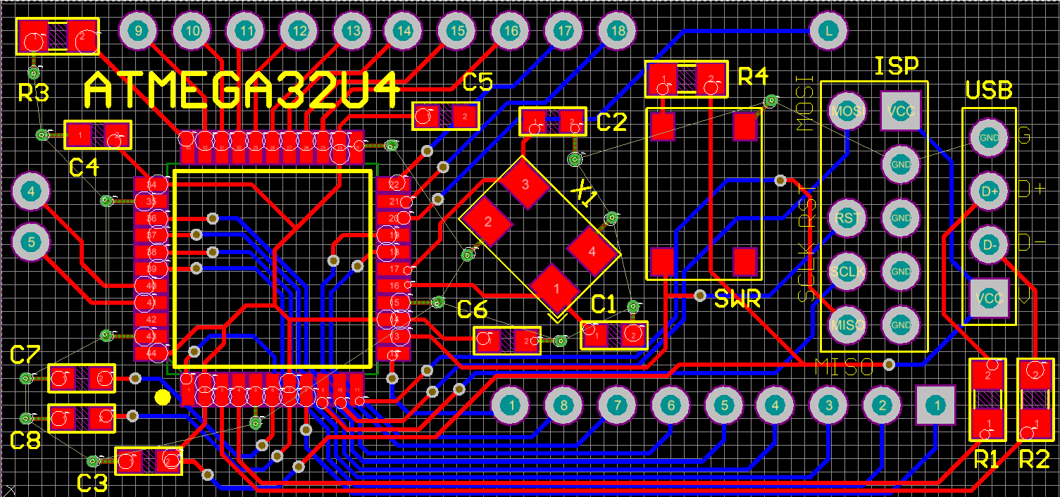
1- in Ruiqi Mao’s guide, pin 33 (PE2) is connected to a 10k resistor and then to GND, why is that? does this pin have a special functionality?
2- the ISP pins are SCLK, MOSI, MISO, RESET, GND, VCC
is this correct?
3- with the ISP pins, I will be able to install bootloader without having to use an expensive “socket”, is this right?
4- I wiill be grateful if someone can give me a review on my board.
If you look at the ATmega32U4 datasheet (pages 3 and 81), you’ll see that this pin is also !HWB, which stands for HardWare Bootloader. So, by pulling this pin to ground,
HWB allows to execute the bootloader section after reset when tied to ground during external reset pulse.
This is the feature that allows you to program your microcontroller without the need of an specialized AVR programmer.
And yes, ISP pins are those you mentioned, and you can use a standard AVR programmer with 2x3 (or 2x5) connectors for that.
I’d avoid that acute angle trace junction near C3, as it is an invite for problems when the board is etching. And while it isn’t a problem, I don’t understand why the trace under SWR is “broken” instead of a straight one.
It’s also highly recommended, although not mandatory, to add bypass capacitors as near as possible to all microcontroller’s Vcc pins. 100nF should do the trick.
oh… silly me, I may have via there… and removed them after.
I will change the line to straight one
is it necessary that the traces to bypass capacitors to have roughly the same length? (similar to traces to the crystal)
(from Ruiqi Mao’s PCB Design Guide)
Now the most important part of PCB design: the crystal. We need to make sure the traces to the crystal are as short as possible and that they are roughly the same length
Hi Tom, nice work so far! One comment I have is that I think it’s generally advised to not run any traces under the crystal, since this could interfere with its operation. Here’s a document I found useful about oscillator best practices.