Hello All,
I’m hoping one of the technical wizards on this site might be able to steer me in the right direction. In a couple of other posts I’ve noted that I purchased a mystery Bluetooth, hotswap PCB from Aliexpress and I’ve been trying to make it fit a bunch of use cases that it wasn’t meant to. Most recently I have been trying to get it working in a 3D-printed Bakeneko case I got.
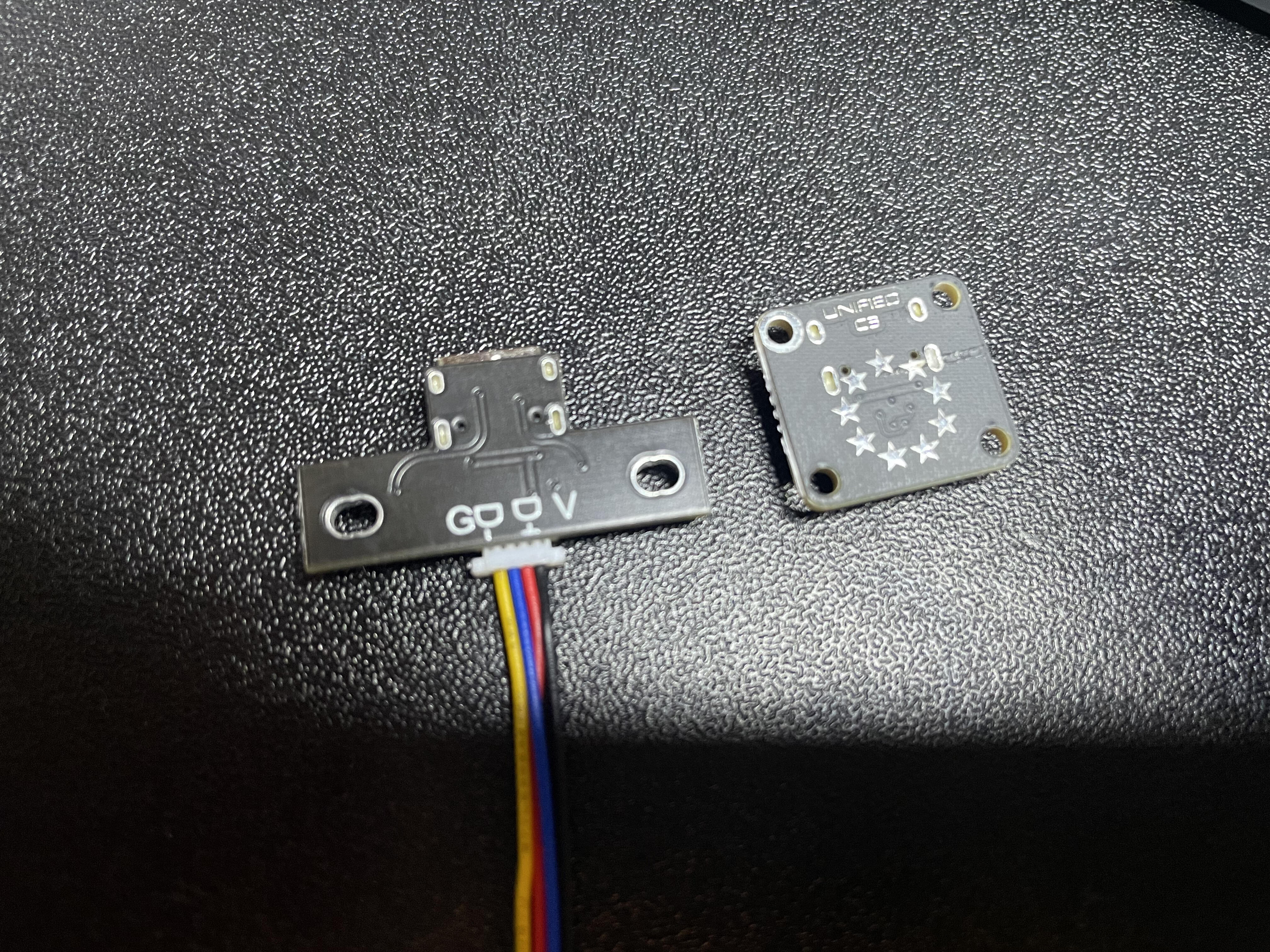
The Bakeneko case is printed to fit the C3 Unified Daughter Board (now considered legacy) in the USB slot. Unfortunately, the PCB came with it’s own daughterboard (different form factor) and it does not seem to work with the C3 Unified DB.
Since it’s just a USB pass-through and they use the same 4-wire JST cable, I’m wondering if it would be possible to use the C3 w/ the PCB by, potentially re-arranging some wires.
Luckily, the makers of the unknown DB screened a “wire guide” on the bottom side of the DB and the C3 board is well documented.
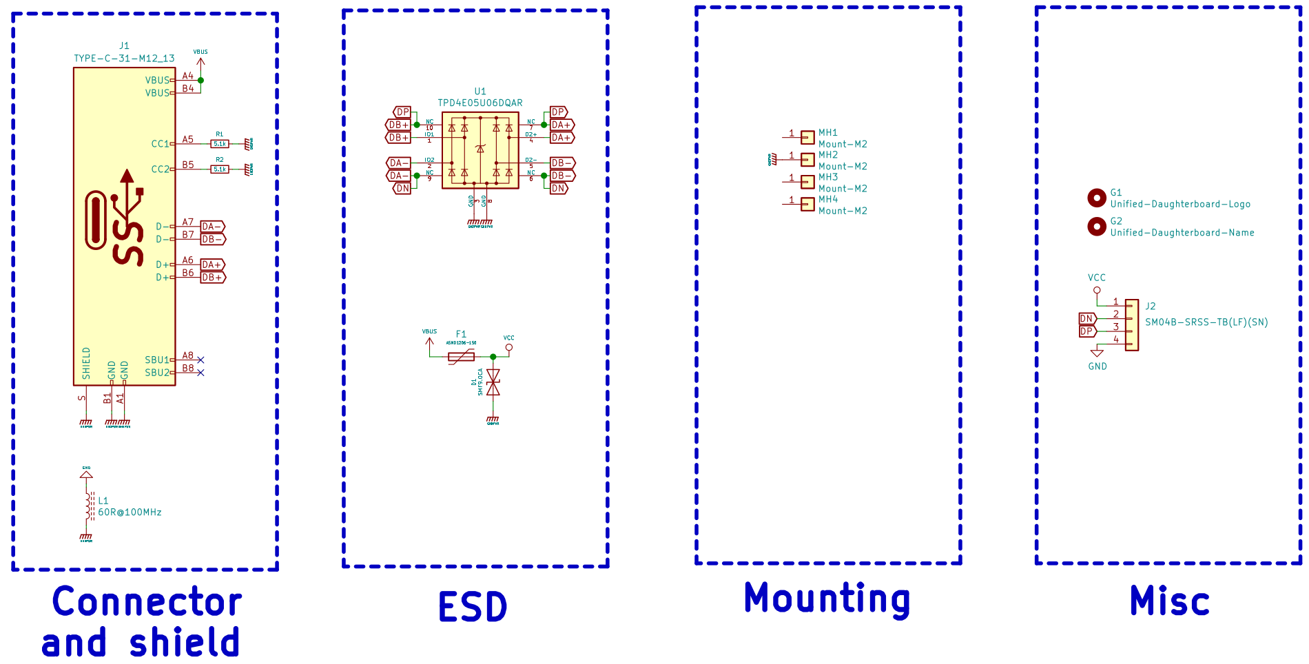
Per the C3 github page it is wired like this:
Two things are unclear to me:
- Does the wiring guide represent a view from the top of the C3 DB, or the bottom?
- Do the DN/DP wires on the C3 wiring guide map to the symbols in the middle two wires on the unknown daughter board?
I’m interested if I could make a custom JST cable that aligned the pins of the PCB to align with those on the daughter board. I don’t quite understand enough about the way that daughter boards work, however, to know if that makes any sense.