(Moderators: Please delete or move the post if this is not the right forum for this kind of question.)
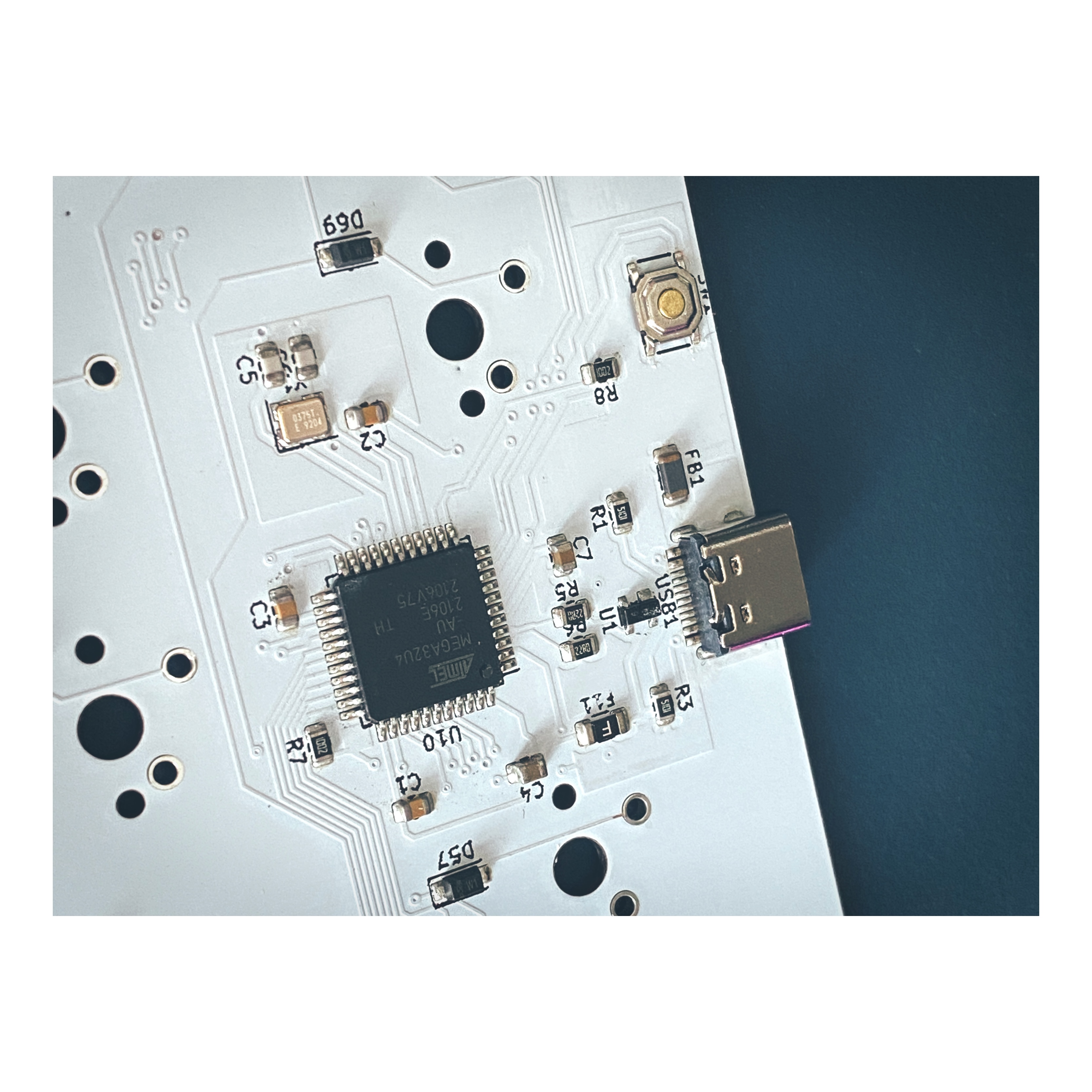
I’m in the process of designing another keyboard and looking for some feedback on the routing and placement of components. I’ve design and built several custom PCBs in the past but I always just did the matrix and then routed everything to the pins of a pro micro, so this will be the first time I’m trying to place all the components on the PCB directly.
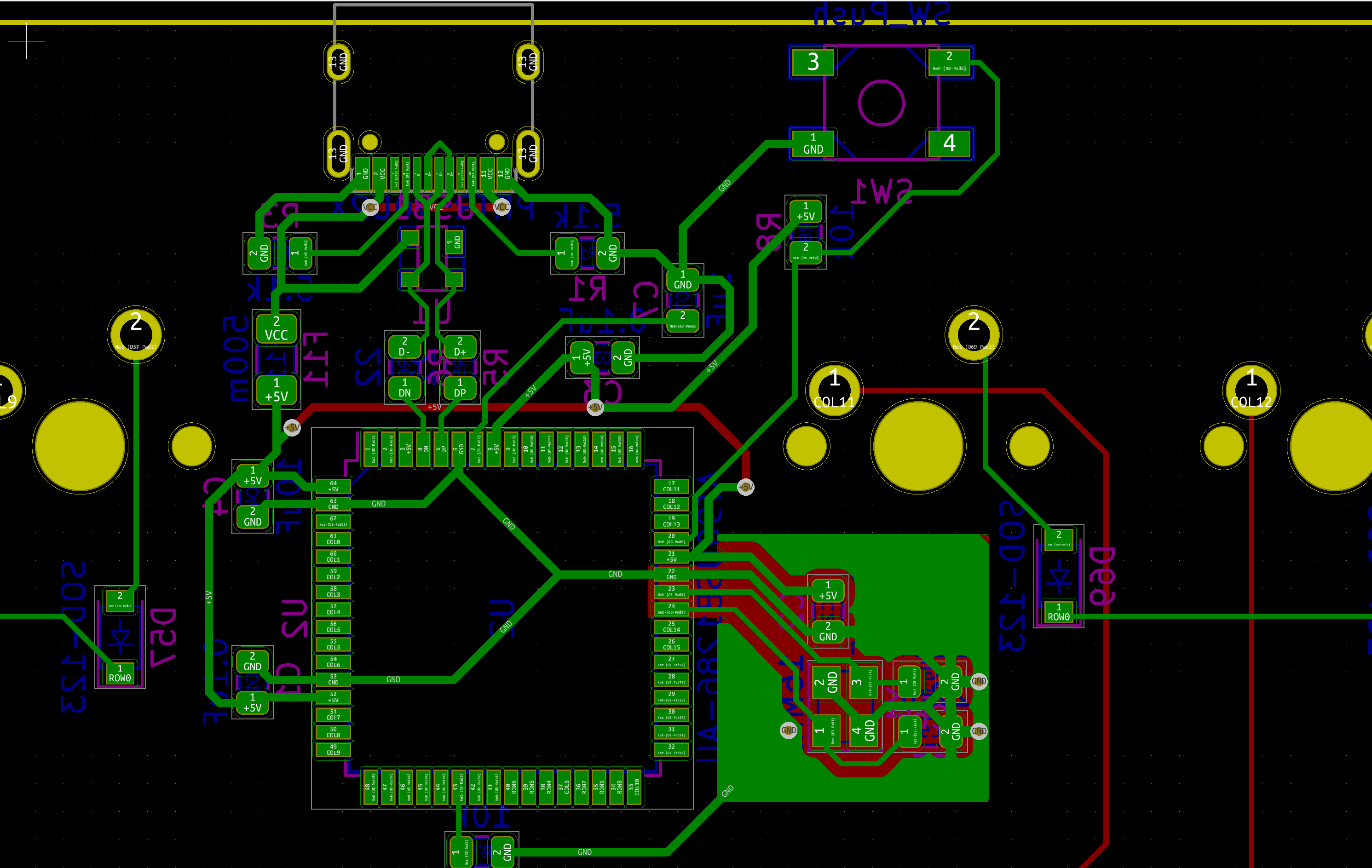
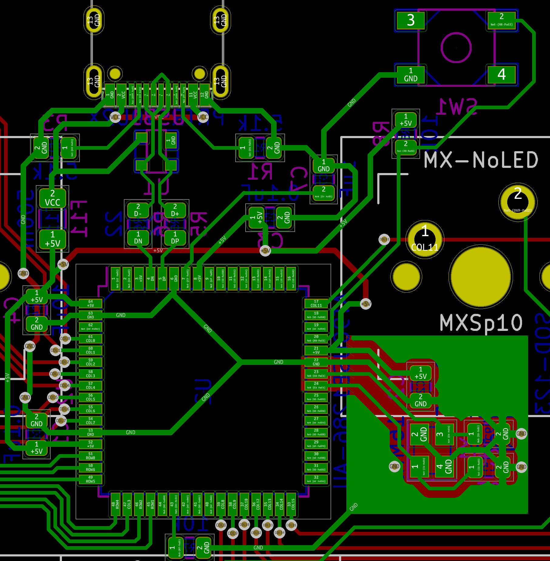
Also, I’m fully aware this might not be the prettiest routing / design, but I mostly just want to know if it is acceptable / would work as is, or if there are any glaring omissions / mistakes. (The switch matrix has been removed for clarity.)
Some explanations:
USB C port on top, with reset switch off to the right
Differential pair of data lines passing from USB through a RtR ESD protection diode, to the MCU
Crystal off to the right
Bunch of decoupling caps scattered around the MCU
Someday I would love to build an actual commercial product but at this point I’m just starting out and learning as I go.
It is difficult to say if you have errors wihout having acces to the schematic and ideally to the project file itself.
To mitigate the risk of errors as much as possible I strongly recommend to regularly do DRC checks on both the schematics and the PCB view(in PcbNew).
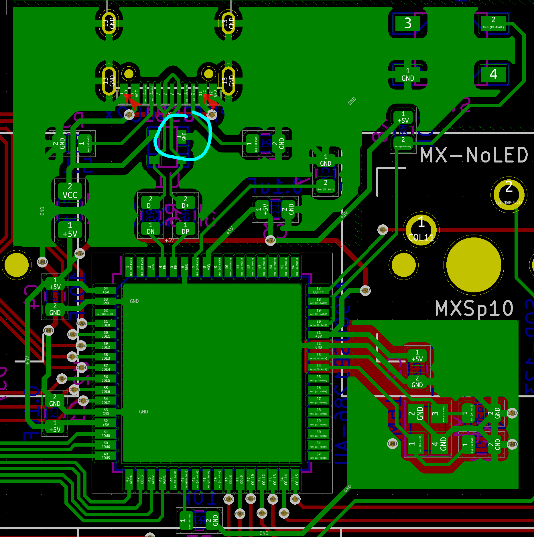
For example it looks that your ESD chip ground pin is not connected to ground. While it should still work it will make ESD protection not working as the goal of this chip is to divert all voltage spikes to ground.
Simple DRC checks will tell you if you forgot to connect pins.
I’ve run the DRC checks in KiCad regularly and it’s not flagging any issues, but I think you are right about the GND pin. Will double check once I’m back in front of a computer.
A common design practice that would have mitigated your ground oversights is the ground plane.
It’s not an intuitive thing to use because in our minds, traces on a PCB are wires and for a ground plane there is no breadboard equivalent. But fear not, KiCAD has great tools for creating a ground plane without any headaches.
Ok, back in front of KiCad. The reason the missing GND net connection wasn’t flagged was because I had added a filled GND zone around the components, and the ESD protection diode got connected to the zone.
(Btw, the two DRC flags you see are warnings that the pads on the USB-C footprint are too close, but this is coming from ai03’s lib so I’m going to assume that the footprint is ok (famous last words…)).
Thanks for the comment! I was literally typing out a response when I saw your note.
I’ll look into the plane as well, but I wonder if a Zone like the one used here would suffice? Or maybe they are the same thing? (so much to learn…)
Edit: That’s a great link you posted! Thanks for that!
In low data rate applications like a keyboard controller you can get away with many things that would come back to haunt you with more advanced designs. So yes, that ground fill would be sufficient for the circuit to work. It would have worked with traces only as well.
On the other hand, manufacturing a PCB is a subtractive process. The copper layer is there in the beginning and is then stripped away according to your drawings. So there really is no good reason not to use a ground plane.
Oh and it makes routing quite a bit easier when you don’t have to worry about ground traces. Just leave the GND pads be, draw the ground fill and check for “islands” that might have become isolated by traces that circle around them. Most likely, DRC will spot those for you as well.
If you like, have a look at this application note on USB hardware design and check your layout against its recommendations. Just if you get a kick out of it, because your existing design should be fine for the data rates required for a keyboard.
In general, application notes are great! They are not written by professors but by engineers that use their skills every day. Also, often it’s much easier to learn with a specific problem at hand, where the fun of solving it is motivation in itself.
As said by @APC-7, keyboard PCBs are often very simple and you can get away without ground planes but it makes things much better to route the ground traces with vias.
You can also go further by using a VCC plane below the MCU, this allows to also cleanly route VCC to MCU pins with vias.
I did that on my last design and this allowed me to have no weird traces with vias on the design and looks much cleaner.
This is a technique I learned by looking at Gondolindrim PCB designs, you can check how it is doing by looking at it’s Acheron projects on github, all its PCBs are opensource.
Thank you both for the thoughtful responses, this community continues to deeply impress me with how helpful everyone is. I will definitely take a look at routing using planes instead. Hopefully there are still some learnings in doing it like this once as well .
(And yep, I definitely like geeking out on data sheets / specs and looking at other’s designs, but I don’t really know enough just yet to make sense of it all )
Also something that could be interesting to you about ground planes and other copper fills is that you can play with them to achieve different PCB colors if the solder mask color is not fully opaque (for example green, blue, red, yellow, purple).
In this case, having copper below solder mask will give you the bright version of the color while without copper it will be darker.
For example on my last design I have copper that fills the whole top of the PCB and no copper fill at the bottom. This gives me two shades of green, one for the top (bright green) another for the bottom (dark green).
Be aware that having copper fill on only one side of the PCB makes it warp a little bit during fabrication; it is a known problem (do not know if it happens during copper etching process or during the reflow soldering process).
This is why often people prefer to have copper fills on both sides of the PCB (or even no copper fill at all). Not a big problem though, once assembled with a plate and switches everything is straight again
Haha! Love that! With some clever tracing and layout it sounds like you can achieve some interesting design results! Based on all the advice above I’ve started working on a smaller macro pad to learn more about this. I’ll post the results later
(Side note: I just realized that PCBWay can do Rigid & Flex, which opens up a whole new rabbit hole to explore )
Yep, as long as you stick to parts that are in their lib it is really fast too. You can export a BOM from KiCAD using a plugin they link to from their website.


 (so much to learn…)
 .
. )
)