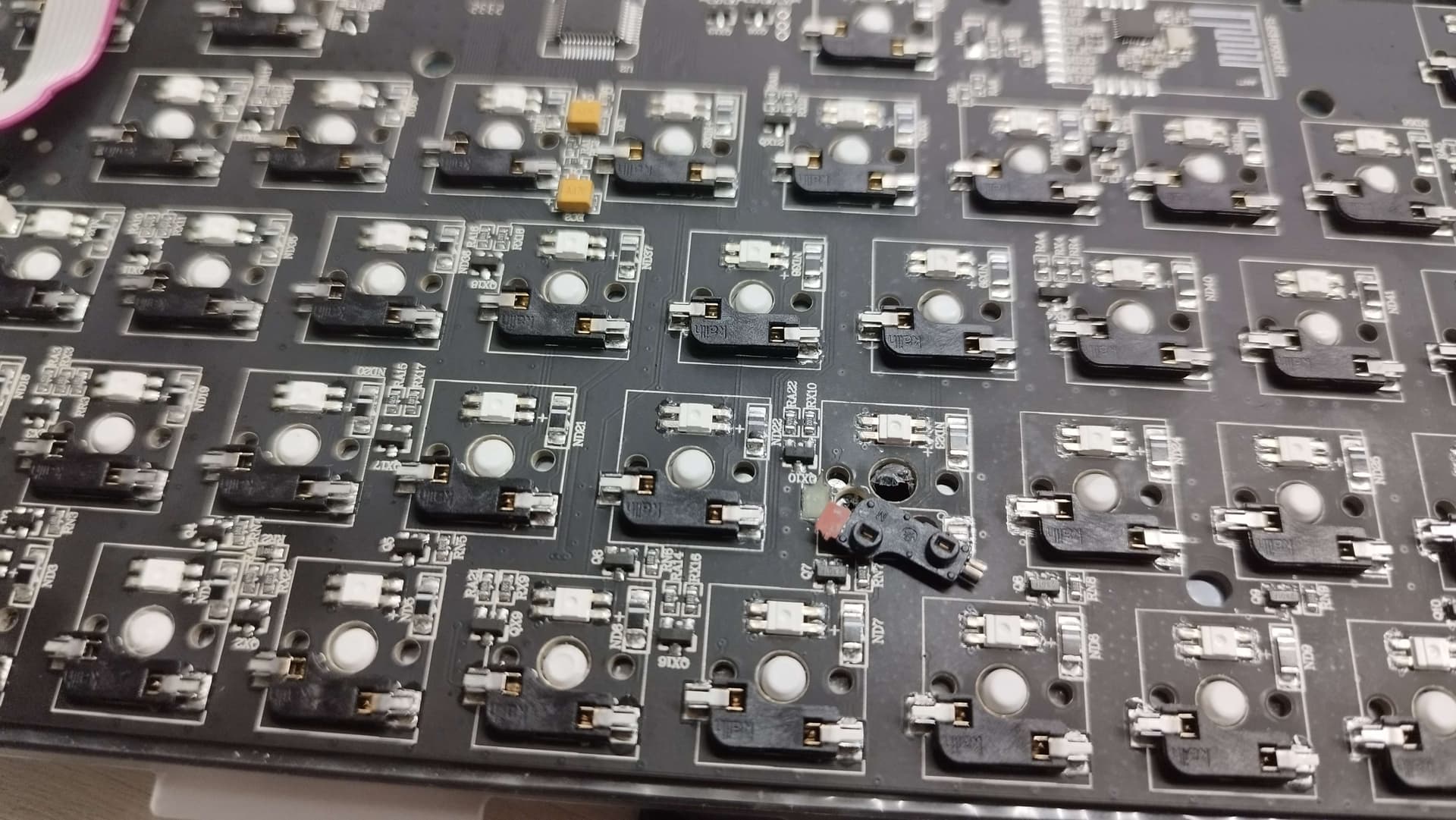
Hello, can anyone advise me on where I should run a wire to fix my kb? (Pls draw a line with MS Paint,) so I can understand better
Thank You so much for your assistance
Hello, can anyone advise me on where I should run a wire to fix my kb? (Pls draw a line with MS Paint,) so I can understand better
Thank You so much for your assistance
I’m not an expert, but I’ve fixed lots of screw-ups. This is how I would go about it:
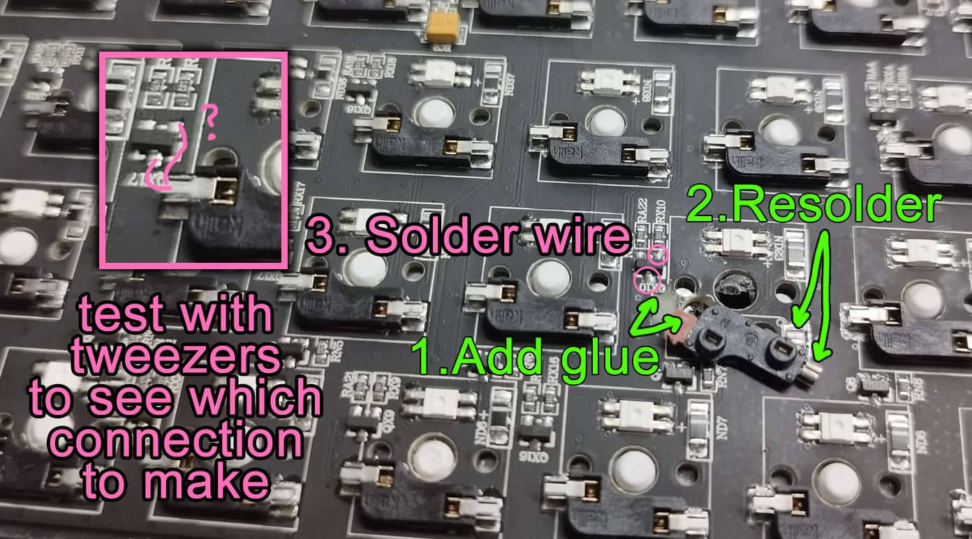
First, you need to get the hotswap socket back in place. The arm on the right can be reattached. Add some solder to the pad on the board and add some to the metal portion of the arm. If you have flux, apply some to the pad as well. Flip it over and put back into place by applying heat to the metal portion. Only 2-5 seconds at a time. You don’t want to melt anything. But right before you do that, you should probably apply some super glue to the ripped off pad on the left. That way you can reglue and resolder in 1 step.
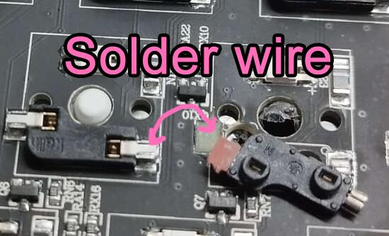
The difficult part comes next. You want to attach a small wire from the ripped off hotswap arm to the diode of the switch. I say it’s difficult b/c I don’t understand this keyboard diode arrangement at all. But I THINK it’s probably going to be one of the pads I circled in pink (you’ll have to open the full size image to see this, perhaps). You can test by holding some tweezers to bridge that connection while depressing a switch inserted to your newly reattached hotswap socket. This can be a task with only two hands. In the past, I have taped the switch stem down so that it stays pressed while I try to use the tweezers on the back. I believe that is a diode that is being shared by two switches. I’ve seen a few like this. Most keyboards used to use 1 diode per switch, but this design saves time and money. But if you don’t get a keypress on either of those two tiny pads coming off that diode, you could try the one above and to the left of your key labeled RX10 (probably the bottom pad, but could be the top)
You won’t hurt anything by bridging a connection between the metal hotswap arm and those diode pads, so probe away.
The transistors (three legged components) are probably to do with the RGB LEDs. I doubt very much they are involved in the switch matrix.
I have annotated this crop from your picture to highlight the traces from the left ends of some of the sockets. They generally skirt the switch leg hole and drop into a via.
This kind of fix is way beyond what I have done with a PCB. If I were you, my next step would be searching youtube for how to solder a patch wire to a via. (videos are better than text and pictures for practical skills)
I believe this is the resistor for the LEDs, right? If that’s the diode for the switch, then it’s a pretty easy fix. It’s a lot easier to just run a wire from the edge of the diode to the hotswap arm than it is to scratch of the solder mask and attach it there. I’ve done this on 2 different hotswap boards. The trouble is always finding where to properly attach the wire.
Surely someone in here knows more about this. It makes sense that the smaller components labeled RA and RX are resistors, since it is an “R”, but what would “N” stand for? And what about QX?
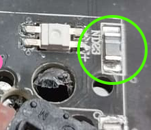
That’s the diode for the switch matrix: there’s a trace connecting the right of each socket to its diode. The pale stripe across one end corresponds to the | in the ->|- of the diode schematic symbol. Dunno what the N is for in the NDxx IDs but the D is evidently for diode.
Alright, so that makes it easier. Apply superglue, reflow right arm, run a wire from the top (or maybe bottom) of that ND23 diode to the left hotswap arm. All fixed! I still have a spare M60-A PCB because I got a free replacement when this happened to mine but I fixed the old one this way.
Nono, only one end of the socket connects to the diode. Each switch and its diode are in series between one of the row lines and one of the column lines, so if the via connected to the left of the socket connects to a row, the other end of the diode connects to a column. (I can’t see which is which because they are on the other side or inside the pcb!) If you wire the left of the socket to the diode, the switch will do nothing.
For pictures and more see ai03’s guide to designing a switch matrix
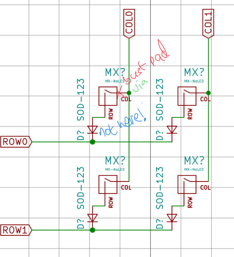
Here’s a wee annotation of how the breakage looks on the circuit diagram, red for the bust pad, green for the via that you need to patch a wire to (sorry if you are colourblind!) and blue for the diode.
See, this is where I just start bridging everything until the correct keypress registers. ![]()
So you would either need to connect to that diode or the diode below/above/left/right of that switch. Get to probin’, right?
Oh, duh, I just realised the patch wire should go to the left end (non diode end) of one of the adjacent switches, if you can’t patch to the via. You can work out which one by plugging in the PCB and using tweezers to bridge from the right pad of the broken socket to the left end of the nearby sockets in turn. When you get the correct keypress you have found a patch wire landing pad.
Yes, I think that’s it! I just looked on my M60-a with a similar problem. With mine, the right side was ripped off, so I just had to connect it to the diode. But since the salvageable one is connected to the diode here, he will need to connect the one with the ripped pad to an adjacent key hotswap arm. Right?
So, possibly this:
Of course, that’s after resoldering the hotswap arm on the right to the PCB, and securing the left one to the PCB with superglue so that future attempts to insert a switch don’t pull it right back off.
No, connecting left and right ends muddles up the rows and the columns.
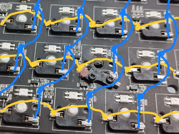
There are roughly two ways the matrix can be laid out, with the diodes connecting the right sides of the sockets to the rows (blue) and the left sides of the sockets connected to the columns (yellow):
Or the right-hand sides and diodes are connected column-wise, and the left-hand sides connected row-wise:
We also don’t know which angle the columns are wired up. But we don’t need to know everything about the matrix, only which of the nearby switches is connected to the same left-hand wire as the broken socket should be.
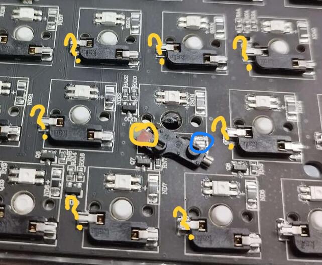
And you can find that out by plugging in the PCB and using tweezers to make a row/column connection as if the switch had connected the yellow and blue circles below. So try connecting the blue pad to each of the yellow question marks in turn. You should find that probably two of the question marks produce the correct character for the broken key.
When you have found a working question mark target, you should solder the patch wire from the left (yellow) end of the broken socket to the working target. Then when the switch is pressed it will make the same connection that you made with your tweezers.
This is interesting.
Thanks for the reply, everyone…