Hi.
I’m planning for a plate mounted, sandwich-type, full ISO+media keys project.
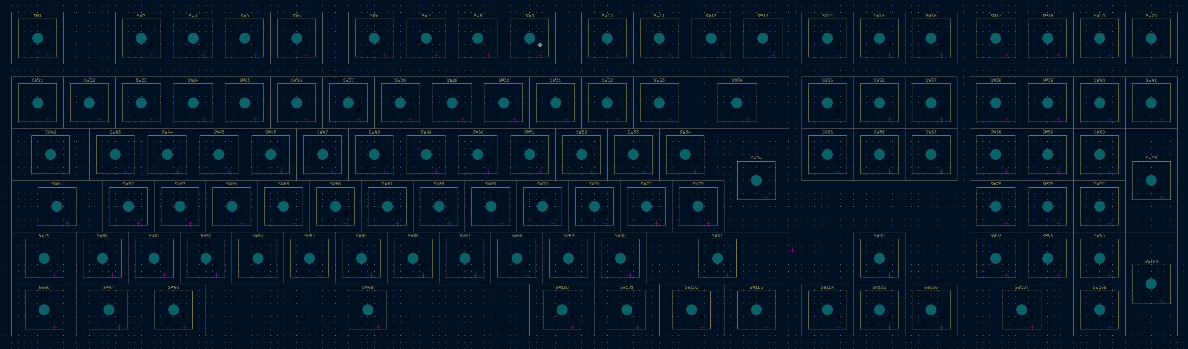
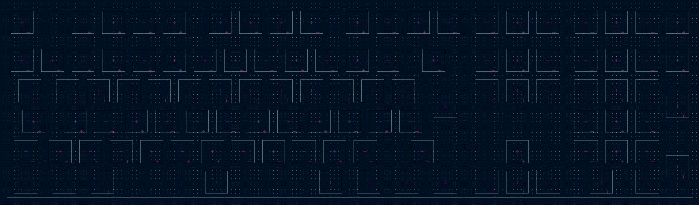
After building my own footprints and symbols to learn more about KiCad, I’ve also been placing the switches without the help of the excellent tool KLE to better understand how key dimensions, spacing and KiCad grids work – as it seemed a confusing mix & match of inches and milimeters.
I think I’ve achieved a decent result there, so now I’ve started adding traces for rows/columns. I still have to route to MCU, place USB, place mounting holes and… well, everything else.
So, before going forward with the hard part of the routing, I’ve thought it would be a good idea to post how that looks so far so I can get feedback about whatever I may be doing wrong.
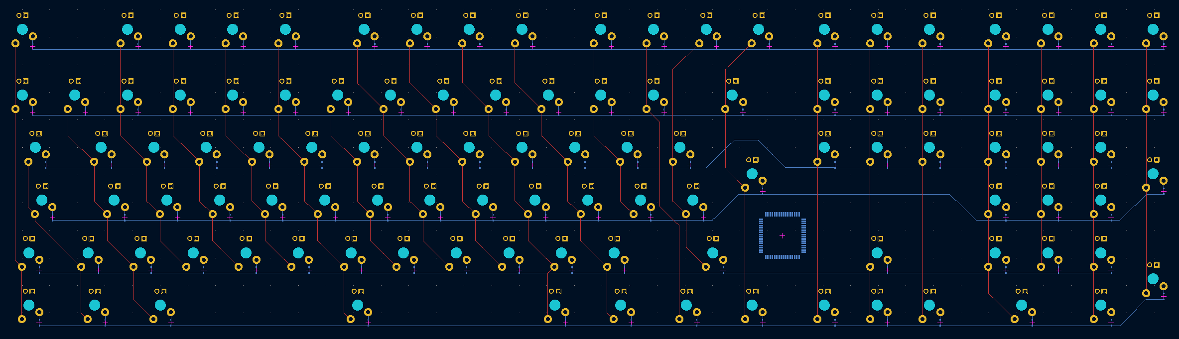
So… this is the picture of the few main traces I’ve laid so far and a temptative placing of the MCU. Do you find something wrong or that I could have been done better for any reason?
Question:
Your switches are north facing, with most of the available switches on the market (there are a few exceptions) the switch top will interfere with row 3 GMK keycaps.
If you plan to use keycaps with see through legends only, having north facing switches is the best option for readability.
If you plan to have light bleeding from the outside of the keycaps only, then maybe go with a south orientation would be better.
Feedback 1:
Diodes footprints looks rather small, but don’t for sure what you used.
If you used SOD323 footprint be aware that it is rather small and a bit of a challenge for starters to solder.
I personally switched to SOD123, bigger and easier to solder.
Feedback 2:
The MCU will collide with the stabilizer holes of the right shift key, it is often placed on top or top/right of the up key for that reason.
Feedback 3:
I’d suggest to make specific footprints for each key size (1u, 1.25u, 1.5u, 1.75u, 2u, 2.25u, iso, 6u and 7u for spacebars).
For keys that need a stabilizer, add the needed holes so that you will easily see if any component you place interfere with them.
I also draw the key boundaries in the ‘user drawing’ layer (a 19.05mm square for a 1u key) so that during switches placement I ensure that I did not made any mistake.
My only reason to use LEDs is readability as I usually work on dimly lit rooms. I pretend to use see-thru-legend keycaps with as less light spill as possible. For this I need thru-hole LEDs and opaque-top switches – Cherry MX Red are my preferred option ATM.
Ideally I’d love to use thru-hole RGB LEDs in an addressable matrix, but options are limited and such a matrix is far too complicated for me right now so I’m going with white LEDs if possible. I have some ideas regarding making some of them addressable to double as indicators.
Keycaps are going to be a nightmare no matter what. For starters, ISO see-thru keycaps for spanish layout are close to impossible to find, and […]
Let’s just say I’ll have to deal with that as a separate issue in due time. Modding a bunch of switches if I need to isn’t the biggest of my worries on that front.
Yes, those are SOD-323 diodes. I’ve been wondering about this too. Apparently I’ll have enough space for SOD-123 which are far easier to solder so I might as well end using those.
I have to say I’m a newbie to building PCBs but not to soldering in tself, though. I was almost ‘born with a soldering iron in my hands’ – I can deal with SOD-923 quite easily… but there’s no point in going small without a valid reason.
MCU was dropped in there just to show it exists! I mean, I still have to find a place for it once the physical/mechanical restraints are set. I was aware of the stabilizer question. In fact I need to ask about that later.
Specific footprints, already done! In fact I also used one more layer when designing the switch footprint to obtain the plate cutout at the same time I was placing the switches – still without stabilizers, though. I hope this way of doing it is accurate enough.
If I may, I’d like to ask a couple more questions.
I’ll be using Cherry stabilizers. I have some dimensional data about them from Cherry, but nothing regarding vertical dimensions like space needed under mounting plate. Any authoritative data on this?
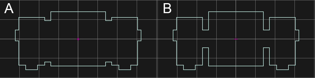
About plate cutout for stabilizers, online tools like ‘ai03 Plate Generator’ give three options for Cherry ones, the classic/spec-following one, and two other rectangular and smaller options. What are the differences? How are the smaller sizes calculated? Which/when should I use any of them and why?
About placing MCU and stabilizers. I don’t like the idea of placing the MCU under an stabilizer… but I don’t really have a logical reason why, is more a general ‘doesn’t look like the best idea’ kind of thing. MCU is going to be, supposedly, placed on the back side of the PCB, so I guess there’s no interference space-wise. Why are MCU not placed under stabilizers then?
If I could, shouldn’t I be placing the MCU closer to USB port if I place this port between the top row keys in order to have shorter and less convoluted signal and power traces? Is the zone around arrow keys or under space bar a bit too far away or it’s OK?
I’m curious about what changes would have you done to the traces I’ve chosen, if any. I have a few places where I’m still not liking it so any comment on this may help me decide.
Make sure you have an edge cut layer set. Sometimes I have thought there was more room then i thought when the edge cut section turned off.
Clearances are setup properly a few traces looked close to the leds.
The diodes apear to be directly on the row truck traces. Technically works but if a pad is pulled it could make the whole row not work.
Rotate numpad enter and plus keys. This is a preference thing for me. As is switches with latch on north and south side then with stabs installed they become tricky to get out.
I’ll be using Cherry stabilizers. I have some dimensional data about them from Cherry, but nothing regarding vertical dimensions like space needed under mounting plate. Any authoritative data on this?
If you are using plate-mounted stabilizers they are already designed for the clearance created by the switches clipped on the mounting plate, so there is nothing to worry about.
Yes, it’s a good one. I know that tutorial, I’m reading that one and many others. What I ask here are things I don’t see clear enough or aren’t explained in a way I can use to understand why.
Oh, about stabilizers. I guessed that might be the case but I’ve taken too many things for granted just to fail miserably that I need to ask, because I can’t find any Cherry document where this is specified.
Visually they surely look like there will be space enough, and logic makes me trust you when you say there’s space enough… but some specifications would calm the itch I feel when I don’t know.
I have edge cut in mind but I’m still thinking about how am I gonna secure the PCB in place besides what the switches will provide. I’m going for a sandwich-mount as thin as I can manage with minimal borders so maybe I’ll go for a non regular rectangle to use the board’s edge to ‘dovetail’ it with a hard wood ‘perimeter’ in-between.
Clearances are something I’m reading about and they apparently depend on manufacturer’s capabilities. So far I’m using 6mil but the closest I’ve gone is double that space from any pad. In any case, this is a first attempt at laying the basic traces but they’re bound to change when I add LED traces, so I still have time to change that if I learn 6 or 10 mils are not enough. Do you think that’s enough clearance?
Diode’s catode pad is exactly on the row trace, you’re right. From what I’ve read and asked, that’s supposedly not a problem but your point is logical enough and I was wondering the same before I placed them like that.
My reasoning for going this way is… if a single key doesn’t work, is a broken keyboard nonetheless, so for me I don’t see that a broken full row can make the keyboard more broken. Also, I’ve seen pads placed like this everywhere, so despite my worries this is apparently widely used – which doesn’t mean is right!
So I’m open to change it if the point you’ve raised is a common consensus or a widely accepted ‘DON’T’. I’m here to learn!
Good point on numpad keys. Didn’t even cross my mind. I’ll have to think about that.
I’m not – generally speaking – thinking about repairing any problematic switch. I’m building my own keyboard with the most standard/widespread parts because of replaceability, so I don’t mind destroying the switch to get it out if I need to… and judging by where they’re placed those may be easier to get out than any inner key.
Then, there’s LED light to consider. I’m aiming for see-thru-legend keycaps. Having a LED on the side instead of north might be not a good solution.
But as I said above, I didn’t even consider this. I’ll have to think it over.
Ignore me on this one. I was trying to give technical advice from my pool deck never a good idea . I went and looked your right this is the normal way.
6ml is good. A couple of the traces by the leds looked close but it is difficult to tell from an image.
Just a heads up this is for pcb stabs not plate ones. I would add the pcb stab hole positions even if you were thing about using plate ones. It is a small change and gives options in the future.
Random kinda tip I found useful is the 3d view alt + 3. For me it helped to space out some of the surface components.
Space between a 1.5mm plate and the PCB is 3.5mm, this is ample space and in general you don’t care unless you are using a thicker plate.
I am not sure, but guessing from the saying I’d recommend the Cherry MX Basis one as it looks to be the largest of the 3.
I really don’t see the point of having super tight stabilizers around the plate, but maybe I’m wrong
People try to find sufficient area on their PCB to place their MCU, and often the easiest spot found is around the space bar.
On a TKL (or full size like in your case) you often place it around the arrow keys, ample space and also closer to were the USB connector is supposed to be.
Obsiously the closer to the USB connector the better, but the main reason is that routing USB data traces (differential pairs) are more complex than for example the row/column traces.
It does look good for me.
The more difficult part remains to be done, that is routing the MCU and the USB lines
Thanks for the feedback.
I assumed ai03 generator was showing 3 different plate mounts but now it makes sense at last.
I’ve modified all plate cutouts for keys that need stabilizer according to Cherry’s specs, though I’m wondering if Bvariation would offer any advantage over A in a 1.5mm thick steel plate.
I’m not going thicker than 1.5mm so no issue, then.
Regarding stabilizers, thanks to @Dave I’ve realized that only one of them was meant for plate mounting, the one that follows Cherry specs, so that’s solved too.
What I meant by “Why are MCU not placed under stabilizers then?” is related to your previous comment about where I placed the MCU, under a stabilizer. If a plate mounted stabilizer isn’t even touching the PCB and the MCU is placed on the back side of the PCB – why shouldn’t I use that space?
About USB, should I give priority to USB signal and power routing over any other trace so they get the better placement possible, then?
And, at last, MCU. I suppose I should start routing once I’ve decided which MCU I’m going to use, shouldn’t I? That’s being a problem given current parts shortage everywhere.
I think I’m going to choose a best candidate and route everything for that MCU, and if the MCU is available once I’ve finished, fine, but if it’s not then I’ll redesign the routing.
I need to advance even if it’s just a provisional result. There’s a lot to do and learn… oscillator, ground planes, minimize RFI…
Which reminds me of another question.
Oscillators. Do I really need an external one if I can find an internal that’s factory adjusted to maybe 1%? I don’t know how much bandwith I need for a keyboard but maybe if I can use low speed I can get away with the intRC. What do you think?
Of course, I could just use the external one… but I like to explore possibilities.
I have not converted over to STM chips yet though I do need to because the Atmega32u4 is old and will eventually move to QMK legacy support.
This article is fantastic read regarding MCUs and admittedly potentially a bit intimidating. All of the acheronproject PCBs are open sourced so you can poke around to find good references for a whole design.
I’ve been reading about it meanwhile and if I’m understanding the whole thing, length is relevant but there’s a small tolerance margin even for differential signal traces. USB sped also dictates maximum length allowed.
It is! Thanks for linking it.
Not really that intimidating but addresses a bunch of questions I had and others I didn’t knew I have. I think it may be useful to me also as an index of matters I need to search and learn – albeit superficially for now.
I’ve also been wondering about ARM core but to my uncultivated neurons ARM surely looks intimidating.
I’m still learning about the USB protocol myself, and haven’t delved into PCB design yet. But I’ve seen it mentioned a number of places that keeping the differential pairs the same/similar length is important for signal fidelity. Most of my own applications have involved cutting and soldering wires, but I would guess the same principles apply whether its wires or traces.
Just wanted to say thank you as well for asking some really good questions in a clear and concise way (and to @Rico and @Dave for the thoughtful and informative answers!). I’ve learned quite a bit from this thread!
 – I can deal with SOD-923 quite easily… but there’s no point in going small without a valid reason.
 I mean, I still have to find a place for it once the physical/mechanical restraints are set. I was aware of the stabilizer question. In fact I need to ask about that later.