I’m trying to understand very basic questions that have been answered a thousand times but in a way I don’t get or maybe I’ve read too much for my own good and now everything is a mess because I lack the education to grasp them.
So, If you allow me asking them, I’ll probably be asking here from time to time.
I’m starting with the keyboard matrix, rows, columns, inputs, outputs, low, high, Hi-Z and whatnot.
I’ll describe what I’ve understood so far – which doesn’t mean I’ve understood it right, so please correct me where I’m wrong.
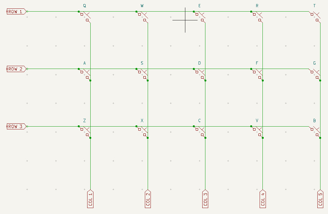
As you see, the customary matrix, without diodes yet.
Now… if I’ve understood it right, because MCUs use pull-up resistors, an “active-low” method is used. The consequences of this are being difficult for me to understand.
So, outputs are all set to HIGH and are driven LOW one by one to sequentially read inputs to find which one is also LOW, what means a key is pressed.
But… at what state do the inputs start? Are they also driven HIGH or left alone in undetermined state (Hi-Z?).
Also, about current flow and diodes…
Let’s say ROWs are output and COLs are input. When scanning, a switch is pressed and row in LOW state is connected to a column in ¿? state, so…
What direction does the current flow? Col to Row?
And therefore, how are the diodes set? Allow current from Col to Row?
Could somebody please clarify this to me? I can’t get my head around this.
This is never easy at first and you have to look at QMK source code for example to see what is really done.
On your schematic the current will flow from col to row.
QMK calls that COL2ROW for the diode direction, and that also means that current flows in that direction because diodes block current flow on their opposite direction.
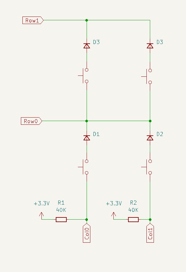
I schematized a simple 2x2 matrix with diodes in it below.
The diodes can be placed before or after the switch depending on your liking (I placed mine after the switch).
Col0 and Col1 IO pins are configured in Input mode with the integrated pullups activated.
I schematized the IO pins pullups with R1 and R2 to better understand how it works.
Of course those pullups resistors are internal to the MCU and you don’t have to add them in reality in your schematic, it is just for understanding.
Now how QMK does its matrix scanning for the COL2ROW case.
Initilialization (called only once):
All col and row IO pins are configured as Input with pullups activated.
In my schematic case those are Row0, Row1, Col0 and Col1.
Matrix scanning:
For each IO row pin(Row0, then Row1):
Configure row IO pin as output.
Set row IO pin in a low state (0) so that it sinks current.
Wait a little bit (QMK default is 30 microseconds).
For each IO col pin (Col0, then Col1):
Read pin.
If it is high, that means that the switch is opened and that the current flows from the pullup to the col pin.
If it is low, that means that the switch is closed and that the current is sinked by the row pin, no current flows to the col pin.
Of course it does!!
Thanks for taking the time to draw it and explain it in detail. Thanks to you many related deductions I made have been confirmed and/or ruled out.
Though I wasn’t specifically asking about QMK, using it as an example and explaining how its scanning works clarifies both diode direction and how it manages pin states.
So… Cols are always set as input… but why are Rows set as input initially and after each “set Row to output-low” iteration?
Also, those 30μs seem too short to be debouncing time so I am I right assuming is due to an electronic reason? What is it?
When rows are set to input they have high impedance (high resistance) and don’t sink any current.
And you want only one row at the time to sink current so that you can properly read col input pins for each selected row.
So all row pins are set as input during initialize, and then switched to output and back to input during the matrix scanning.
As you have guessed the 30uS (overridable in QMK) is not for the debouncing process, it is just a mall arbitrary time for current to settle and be in a stable state before reading the col pins.
This value is very large for that purpose, it could very well be under 1uS and it would still work.
But if you take a 6 rows matrix this translate into only 180us time wasted for waiting, still very short compared to the time of the debouncing process.
As for the debouncing process, it is done outside the matrix scanning (in QMK, but most probably on other keyboard firmwares as well) and as standard value often 5ms is selected.
That means that your computed will see a key press/release change only after that time (plus the time taken to scan the matrix and time to execute the whole code).
This debouncing time is the major factor of keyboard delays.
I need to learn a lot more about electronics+MCUs to fully understand this if I’m to write firmwares that doesn’t fry the ICs.
So…when a GPIO pin is set to input then it’s set to high impedance (Hi-Z ?), so its voltage “floats” at residual value, and then internal pull-up resistor is activated so the pin doesn’t “float” anymore. Is that so?
If I’m right so far… is setting a pin to “input” and setting it to “high impedance” the same thing, or is one of them a consequence of the other?
In other words, do you set the pin to high impedance and it becomes an input, do you set the pin as input and this causes it to have high impedance, or both are the same thing but we use the term “input” to have a better/easier mind map of the MCU?
Thank you, once again, for your patience and answers.
Any advice about where could I find a deeper explanation for those of us with very basic previous knowledge?
Oh, and a final question. I’ve been wondering about how you placed the diodes. I’m assuming you simplified in order to make it easier for me to understand, but now I have this doubt about diodes placed in series.
Unfortunately there is no common place to find every information possible, Google is your best friend.
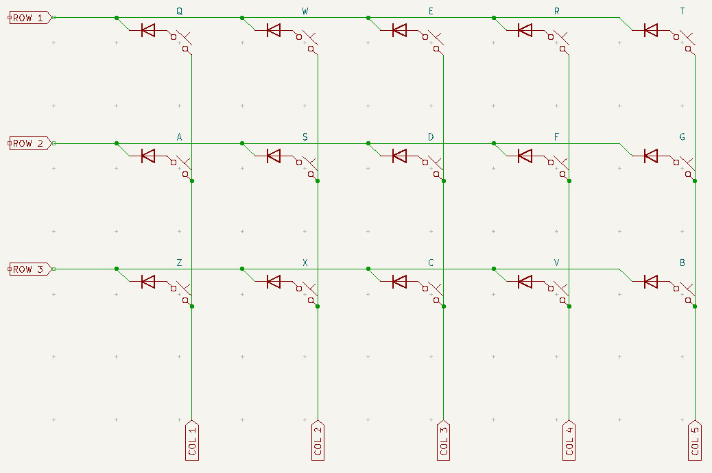
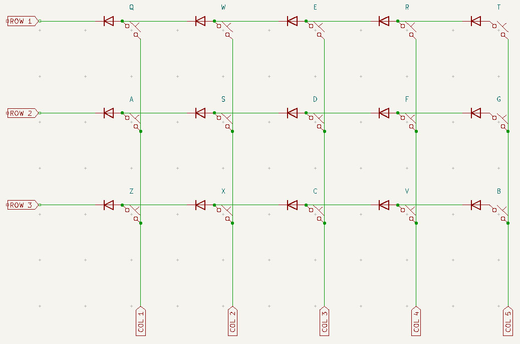
Pic A is the correct way to do.
Pic B will not work.
For example for Col5 pin, the signal will have to travel through 5 diodes, each time with an associated voltage drop. That translates to 5 x 0.6V = 3V, meaning that the rows will never see any high signal from this col.
That’s what I thought… but knowing so little about electronics I might as well have been wrong, so I preferred to ask now that I found someone willing to help me.
Well, I think that’s all I had to ask ATM. I’m really grateful for all the time and patience you’ve dedicated to answer my questions in such a kind and easy to understand way.