I used the same oackage on its little brother the atmega32u4 MU.
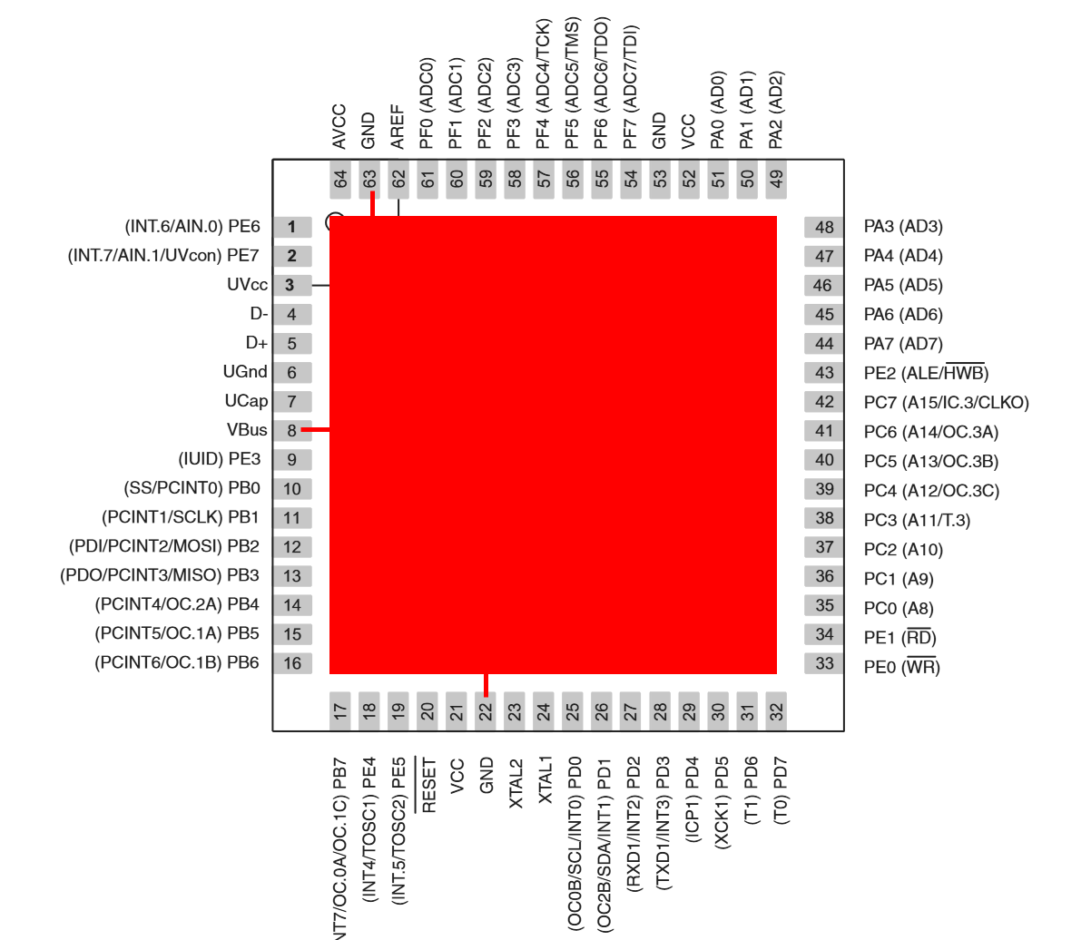
The pad is ground and should be connected accordingly, also it makes routing ground connection very easy.
If you use Kicad footprint, you will see that it will ask you to connect this plane to ground anyway.
As for soldering this thing yourself, If you have a hot air soldering station no problem adding solder paste to this pad, If you use an Iron then you can do without and just solder the outer pins.
ah, thank you!
my ground plane is the layer below (the MCU is in “Top” layer while the ground plane is in “Bottom” layer),
should I put a via here to connect these 2 layers? (connect top to bottom through a via so this large pad will connect to the ground)
or can I connect other GND pads of the MCU to this pad on the PCB?
something like this:
Just connect the pads to the ground plane like you showed in your picture. Adding vias to this ground plane is only necessary when you are dealing with chips that draw a significant amount of current to dissipate heat better (like a led driver for exemple).
i use vias to connect decoupling capacitors to ground, same for crystal load capacitors and crystal ground pins, is much cleaner and more efficient than traces.
Soldering the pad is not mandatory but will give a stronger mechanical bond between MCU and PCB.
Personally I could leave it unsoldered and use only an Iron, easier to deal with.