Hello keeb lovers,
Long time no see in this ‘Making keyboards’ section!
This time it is not for a new home made keyboard case and PCB combo, only a PCB for an existing keyboard.
But what a keyboard!
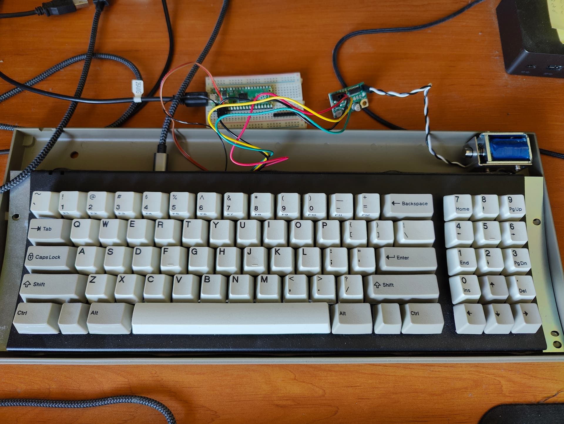
I am talking about the Model F keyboards and specially the F62 and F77 variants that @Ellipse made.
IBM Model F was the predecessor of the IBM Model M, another iconic board that I learned programming on a long time ago.
In term of feeling/tactility the Model F does not disappoint: this is a pure joy to type on, really something that everyone should try at least once in a lifetime.
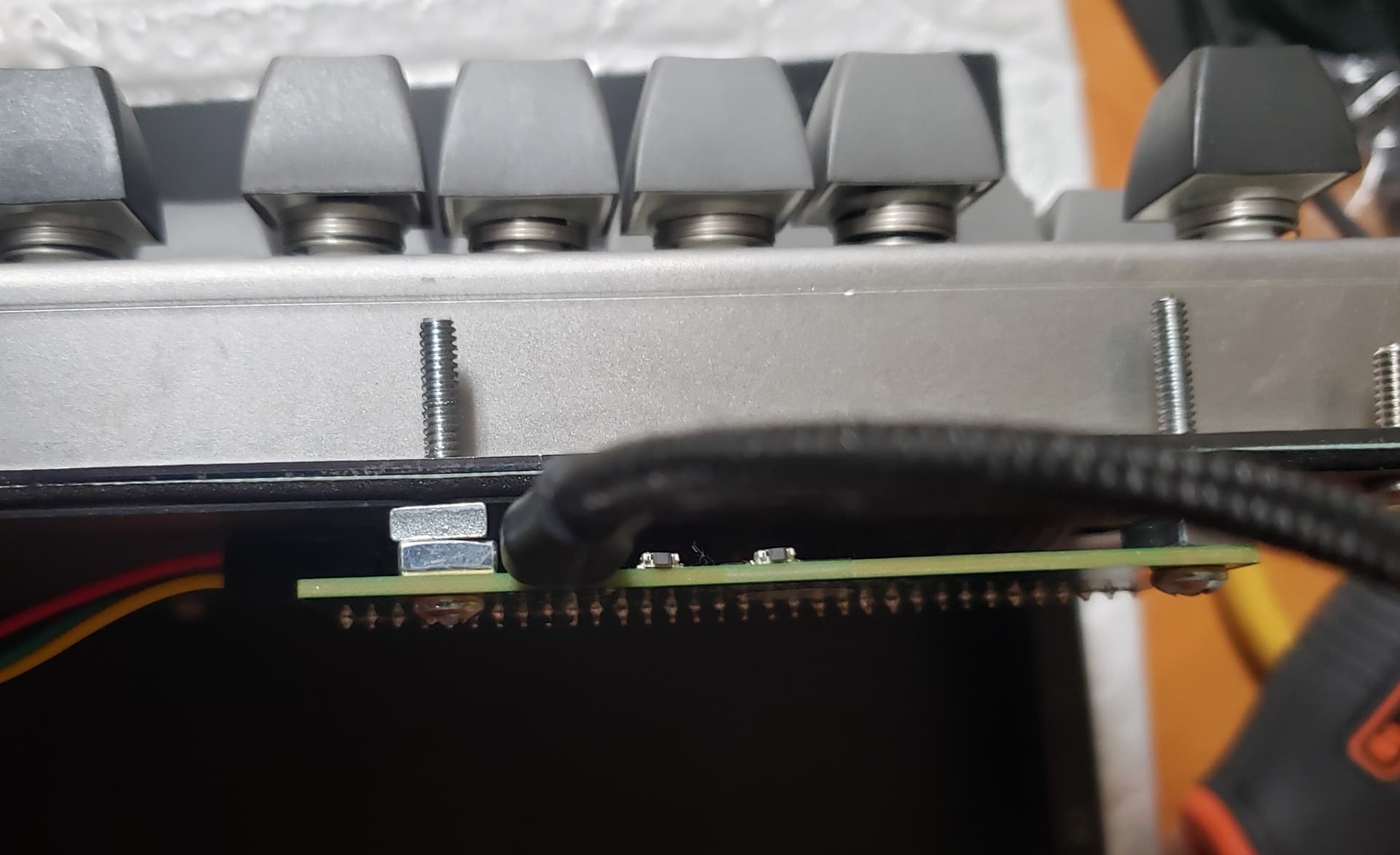
Long before having my own I wanted to undergo the task of making my own PCB for it.
So started to look at various documentation about the electro-capacitive technology behind those boards.
The IBM patents are an interesting read, but the place were I found the most information is on the website of the creator of the original Model-F-USB controllers, Tom Wong-Cornall:
https://static.wongcornall.com/ibm-capsense-usb-web/ibm-capsense-usb.html
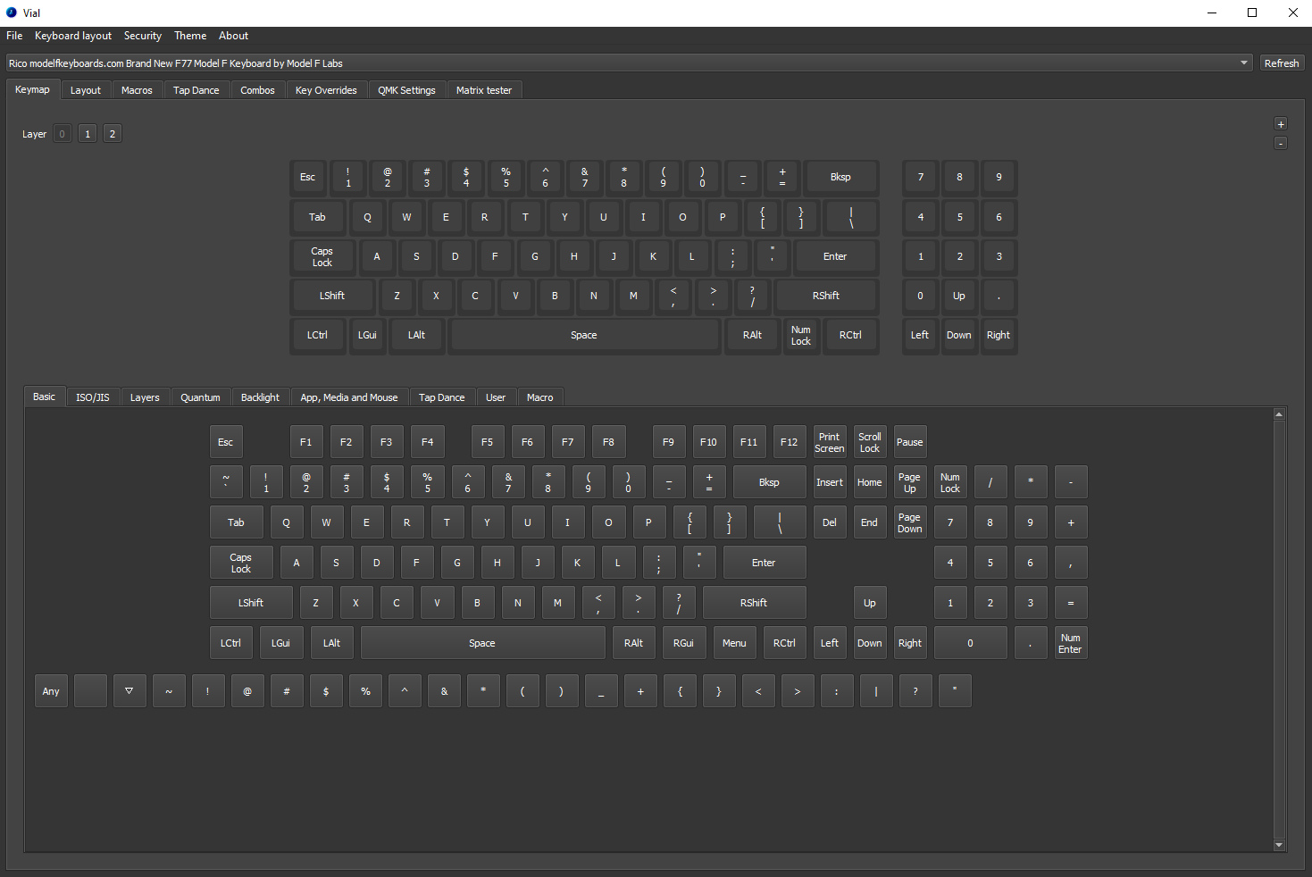
Why making another PCB ? After all there is already a PCB on the new Model Fs that has QMK/VIA support.
The reasons are:
- Not much has improved in the technology behind those PCBs since 2014: most if not all PCBs are based on Tom Wong-Cornall design, up to the components used.
- The small ATMEGA32u2 MCU used in those designs struggle to make everything fit in it’s memory.
- There is a silicon shortage and those Atmel MCUs are now very hard to find and expensive for what they are.
- I want to know if I can do it

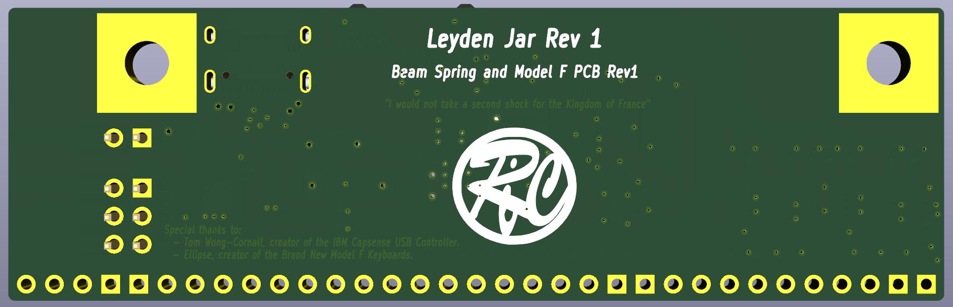
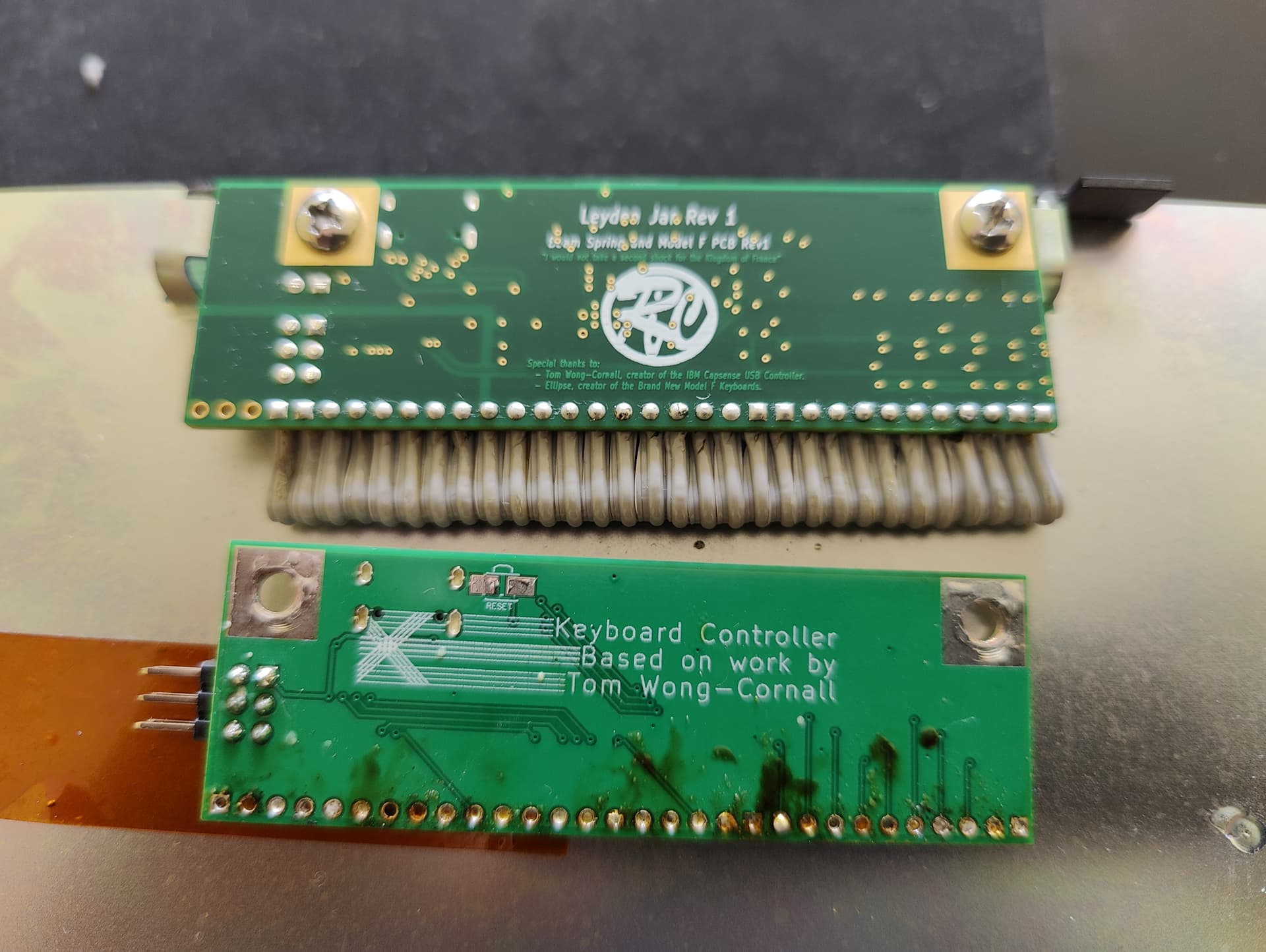
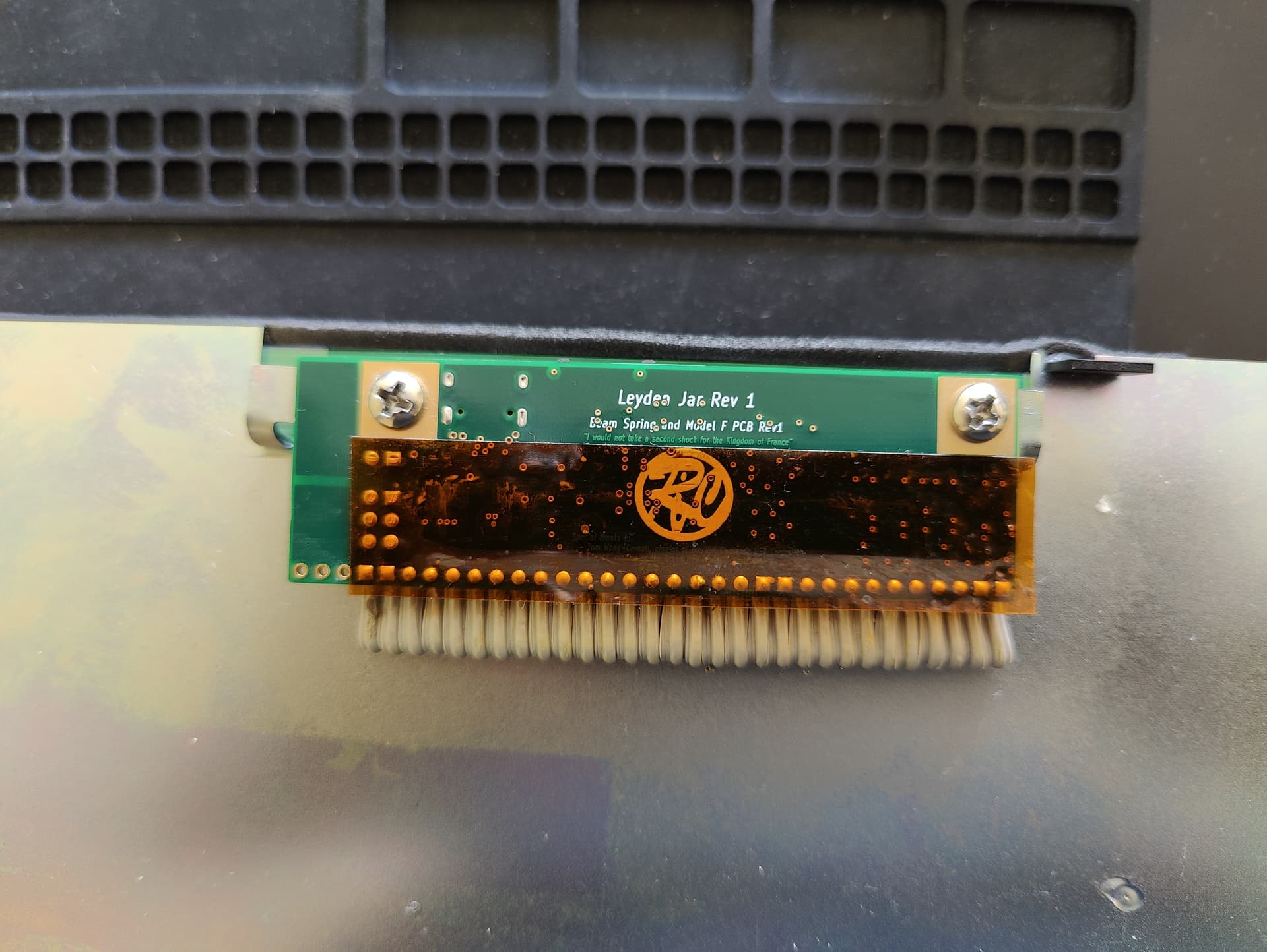
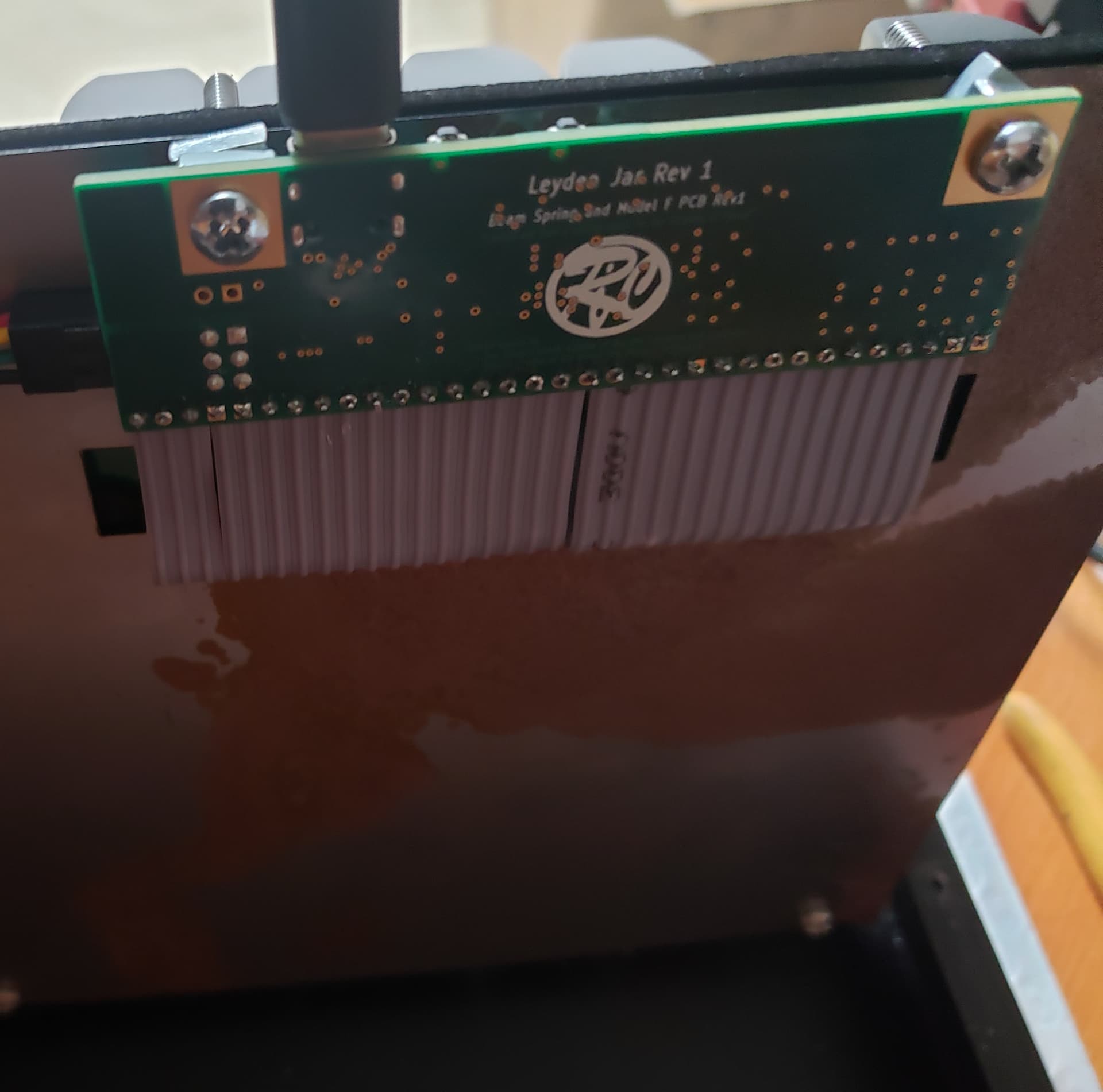
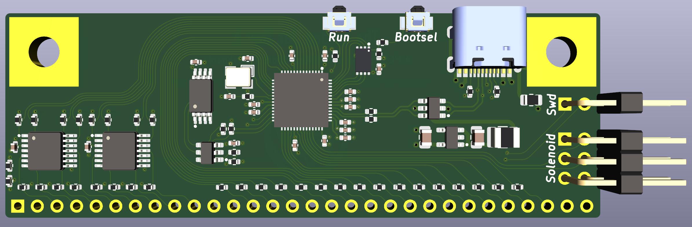
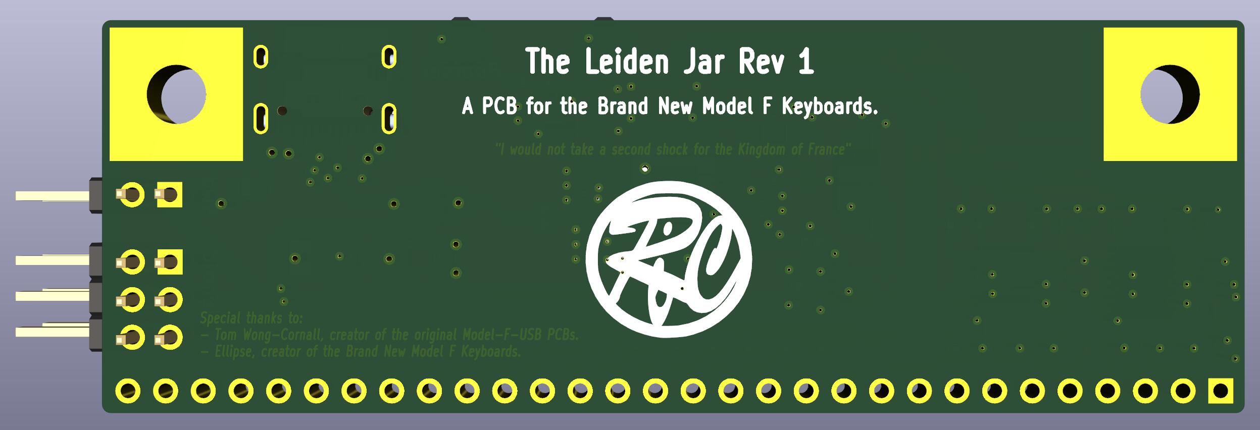
So here we are with the Leyden Jar PCB, name taken from the first ever (crude) capacitor ever invented: Leyden jar - Wikipedia
Some quick specs:
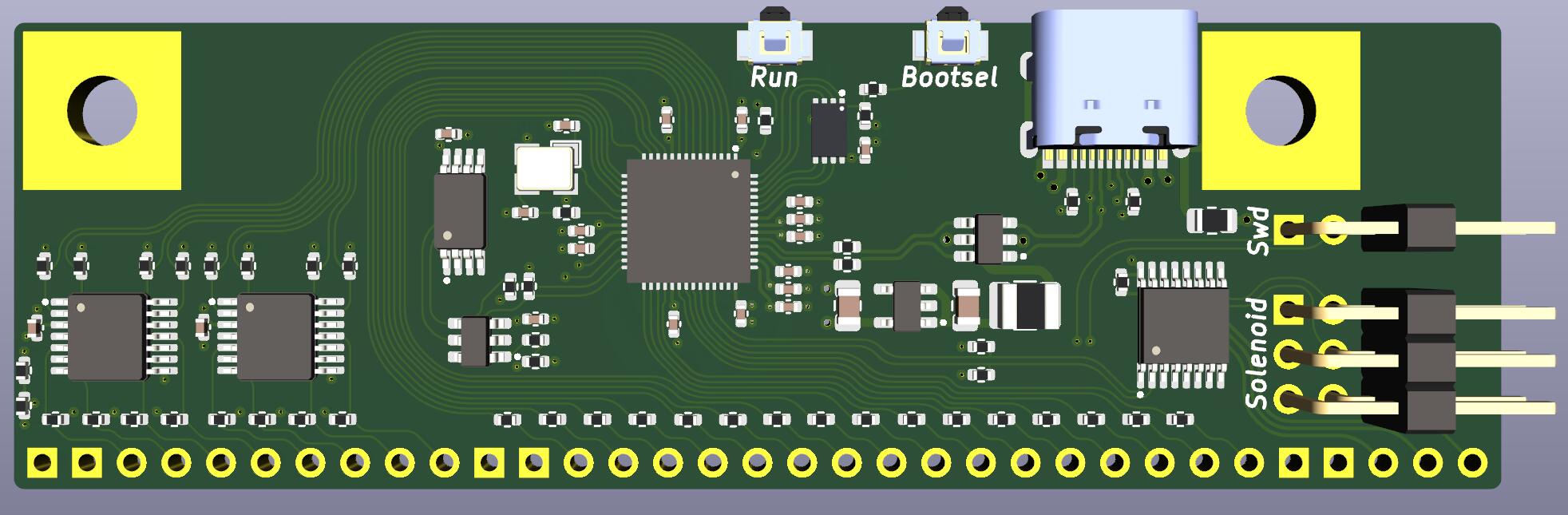
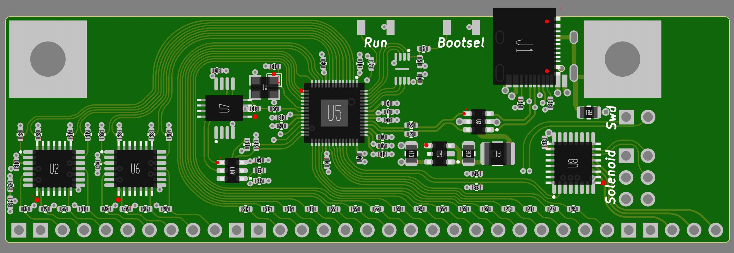
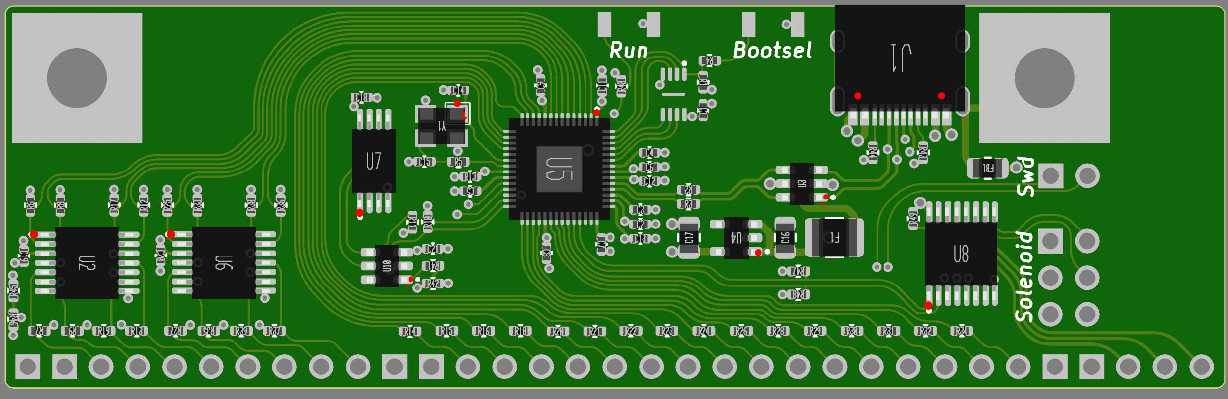
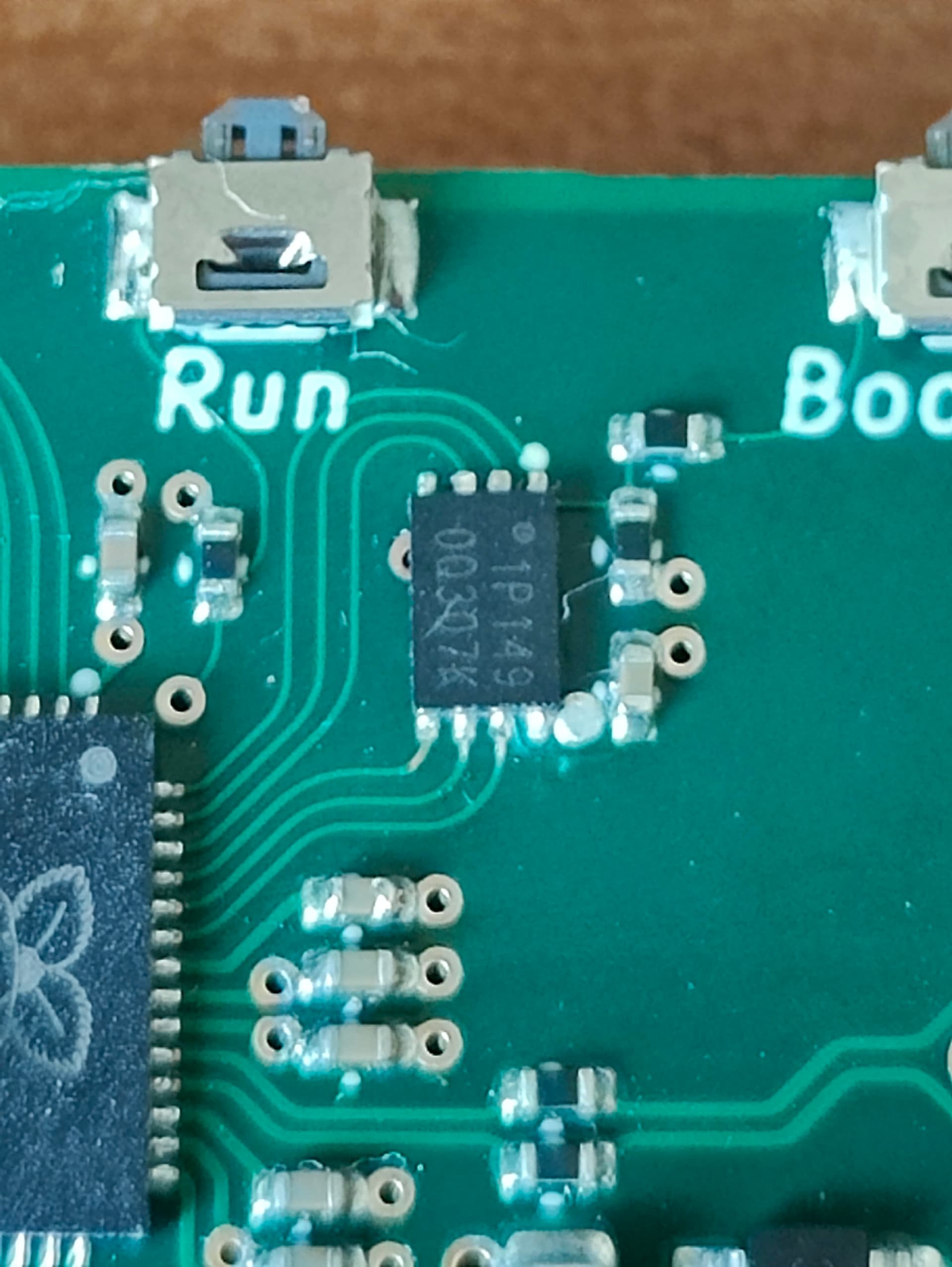
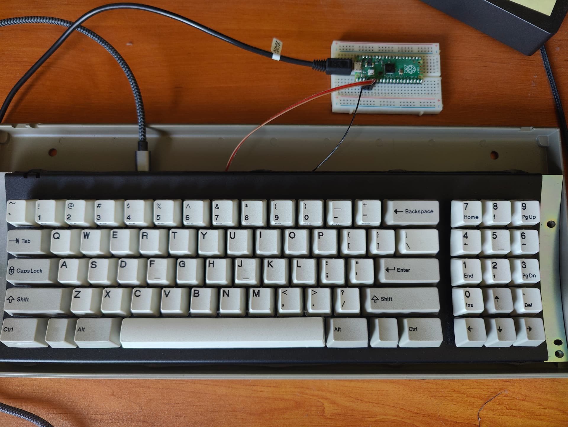
- A modern RP2040 MCU
- Columns directly driven by IO pins (original design uses a IO pin multiplexer that can also work as level shifter).
- Lots of flash storage (16Mbits).
- Lots of EEPROM external storage (512Kbits).
- Uses I2C protocol for EEPROM and DAC chips, saves a few pins doing that.
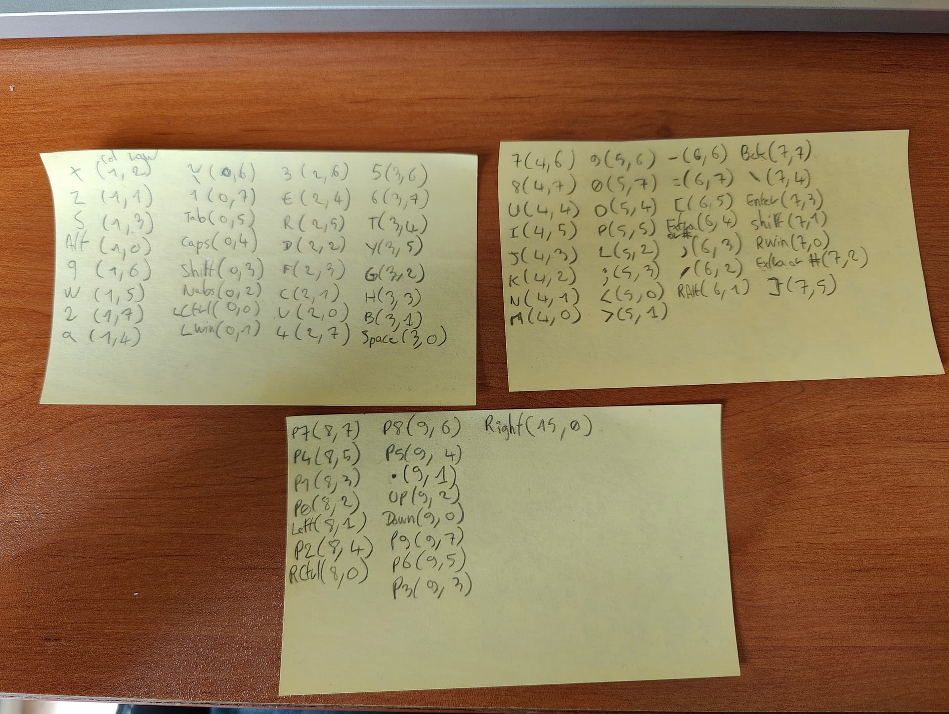
After having seen Gondolindrim constantly use the LTSpice software for simulation, I learned the tool and could make a simulation of a full Model F matrix work.
Without this tool it would have been impossible to find the right technique and components values.
We’ll see how it work in practice but Gondo told me that LTSpice was already giving a good approximation of how things should work(if used well) so I have hope ![]()
There is a lot of things that could go wrong in this design as a lot of things are new to me.
As a result I have a list of stepping stones or goals in mind, so that if the boards is unusable on my Model F I have at least learned something in the process.
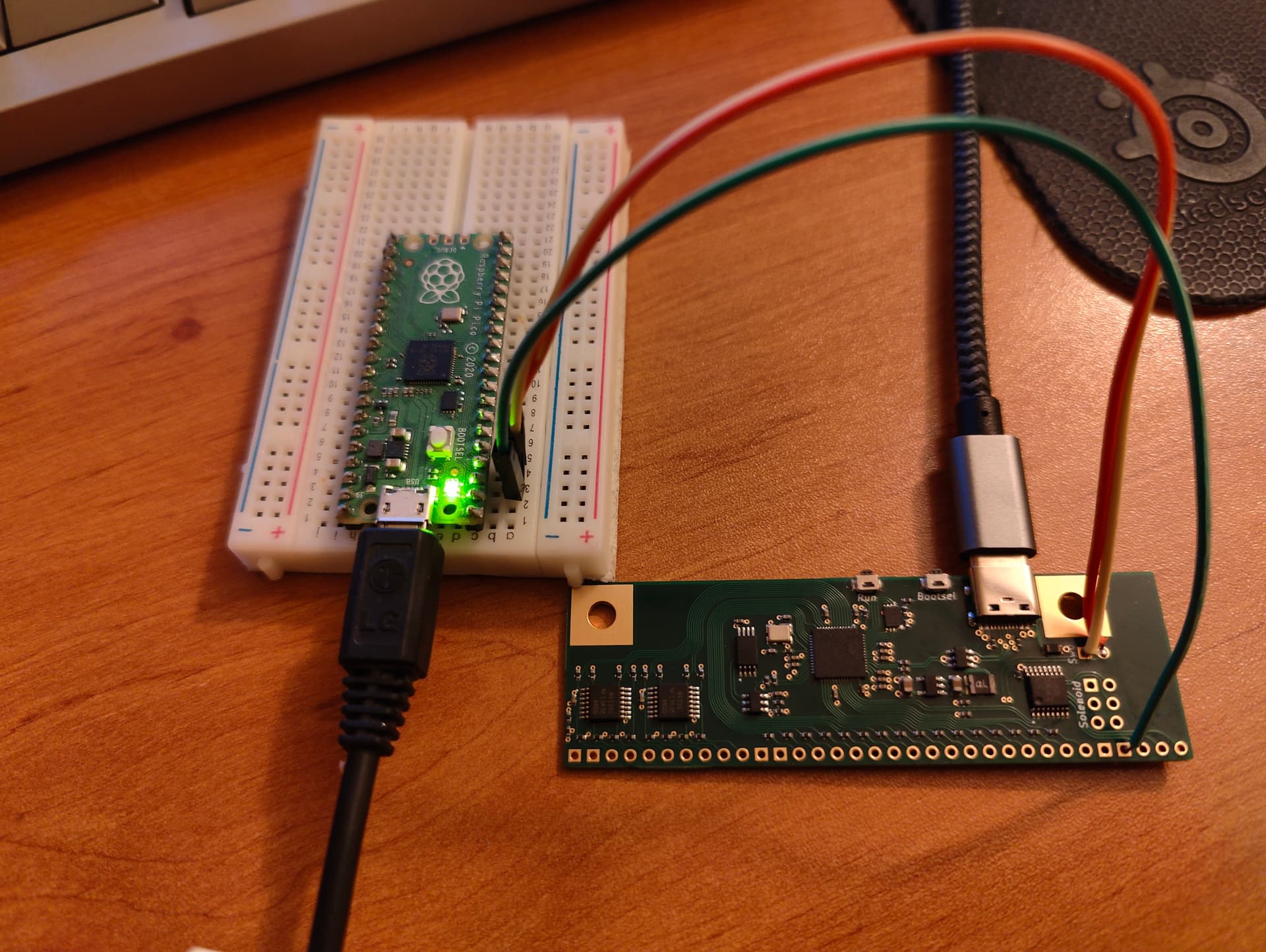
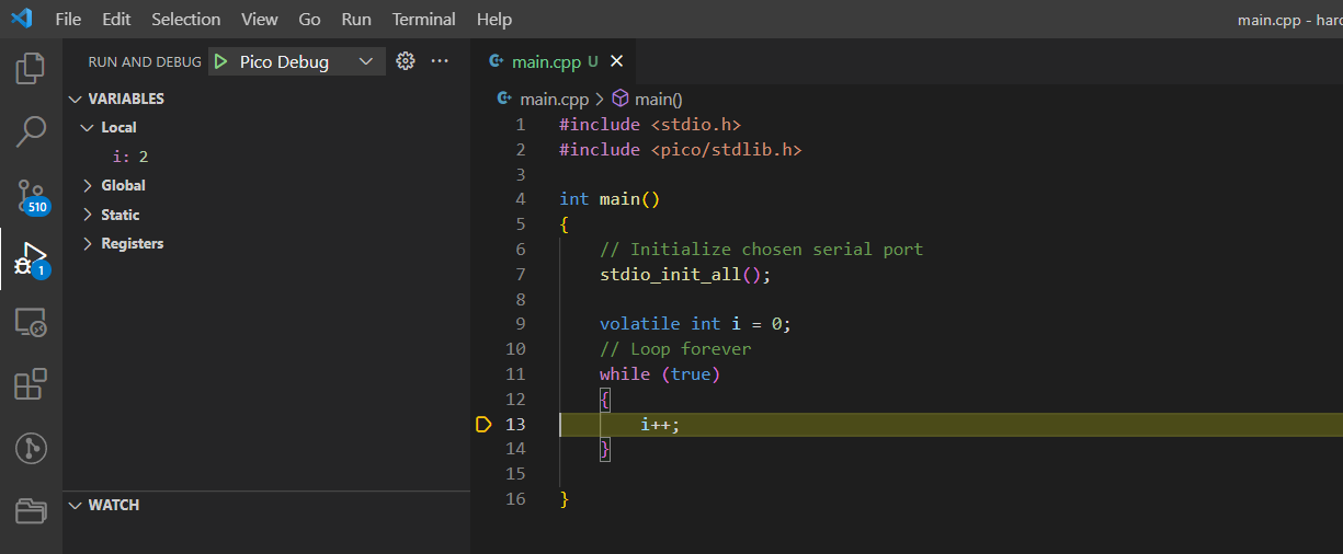
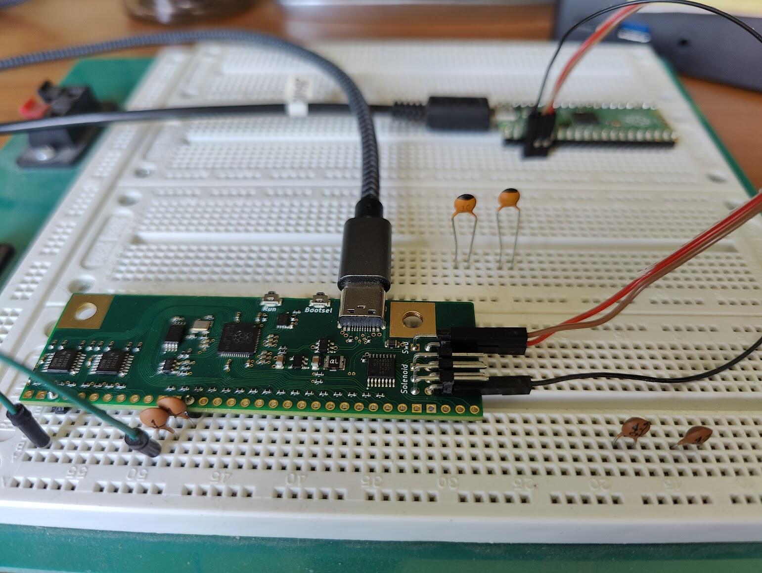
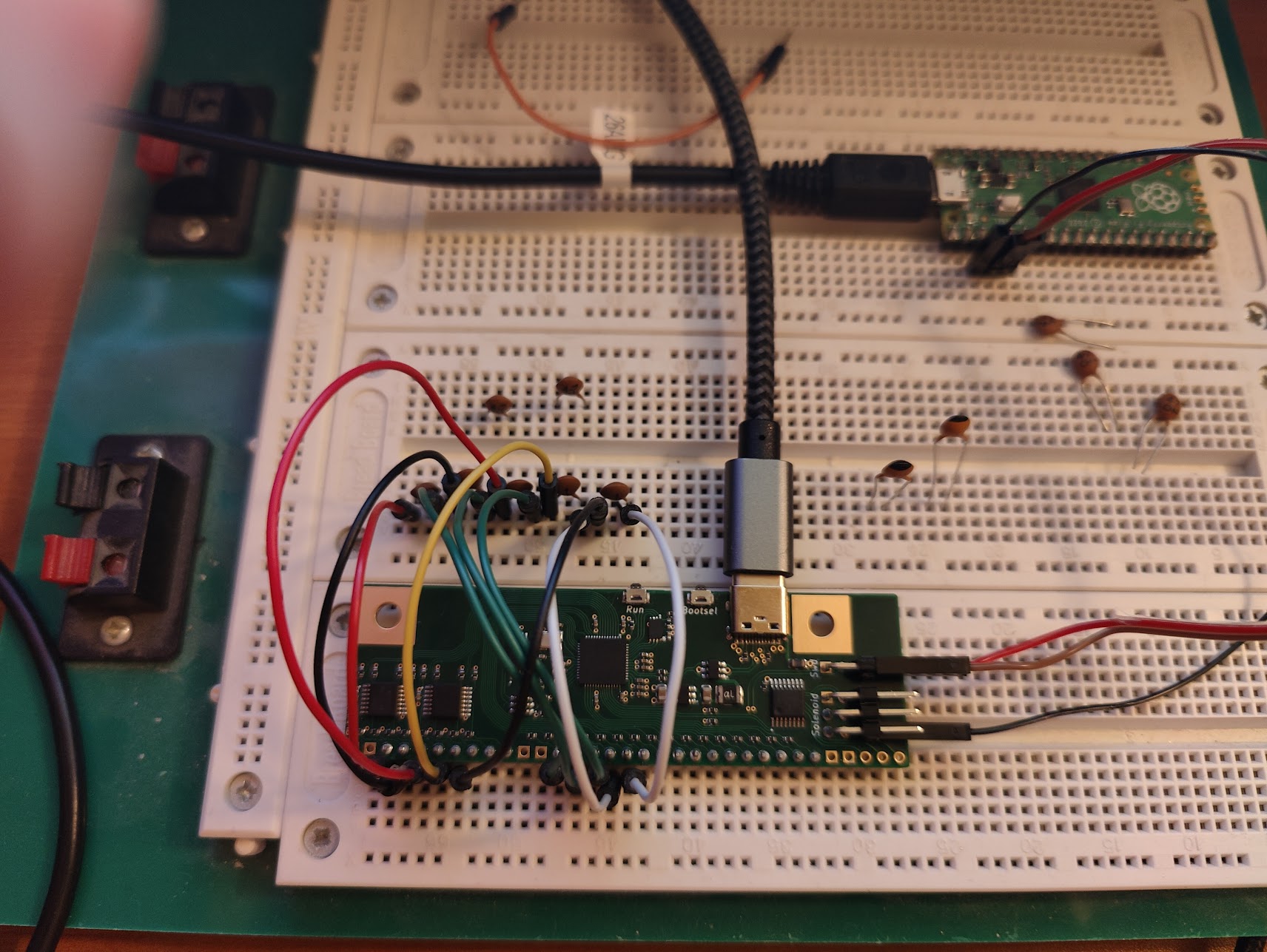
- Have the RP2040 succesfully starting and flashable.
- Can use SWD debugging on it, do the reset circuitry work ?
- Can configure and use the EEPROM and DAC chip through I2C.
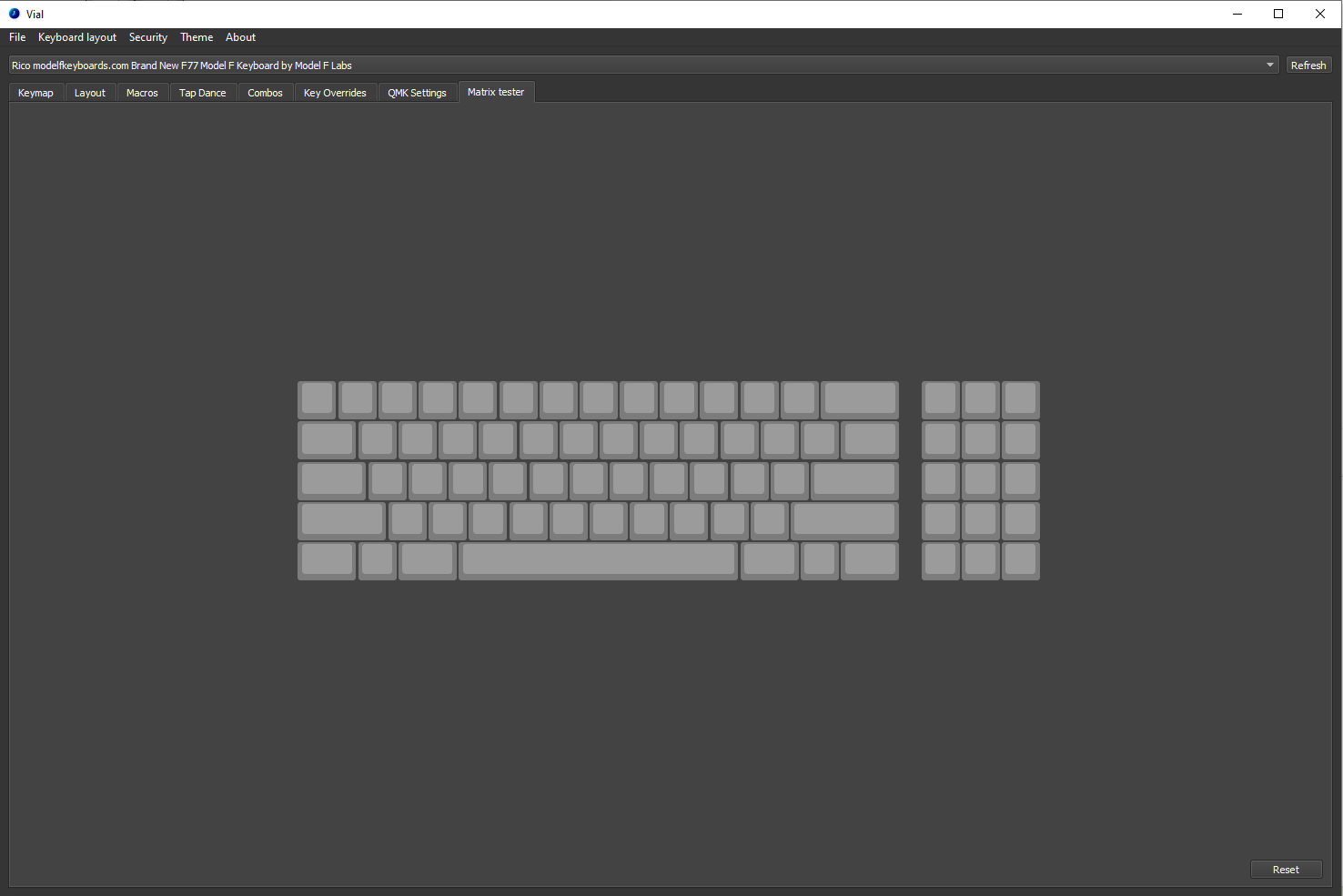
- Can validate that the capacitive sensing works outside of a Model F keyboard.
- Can use one of the QMK fork to have a real firmware.
- Can make the solenoid work (do not have a solenoid at the moment).
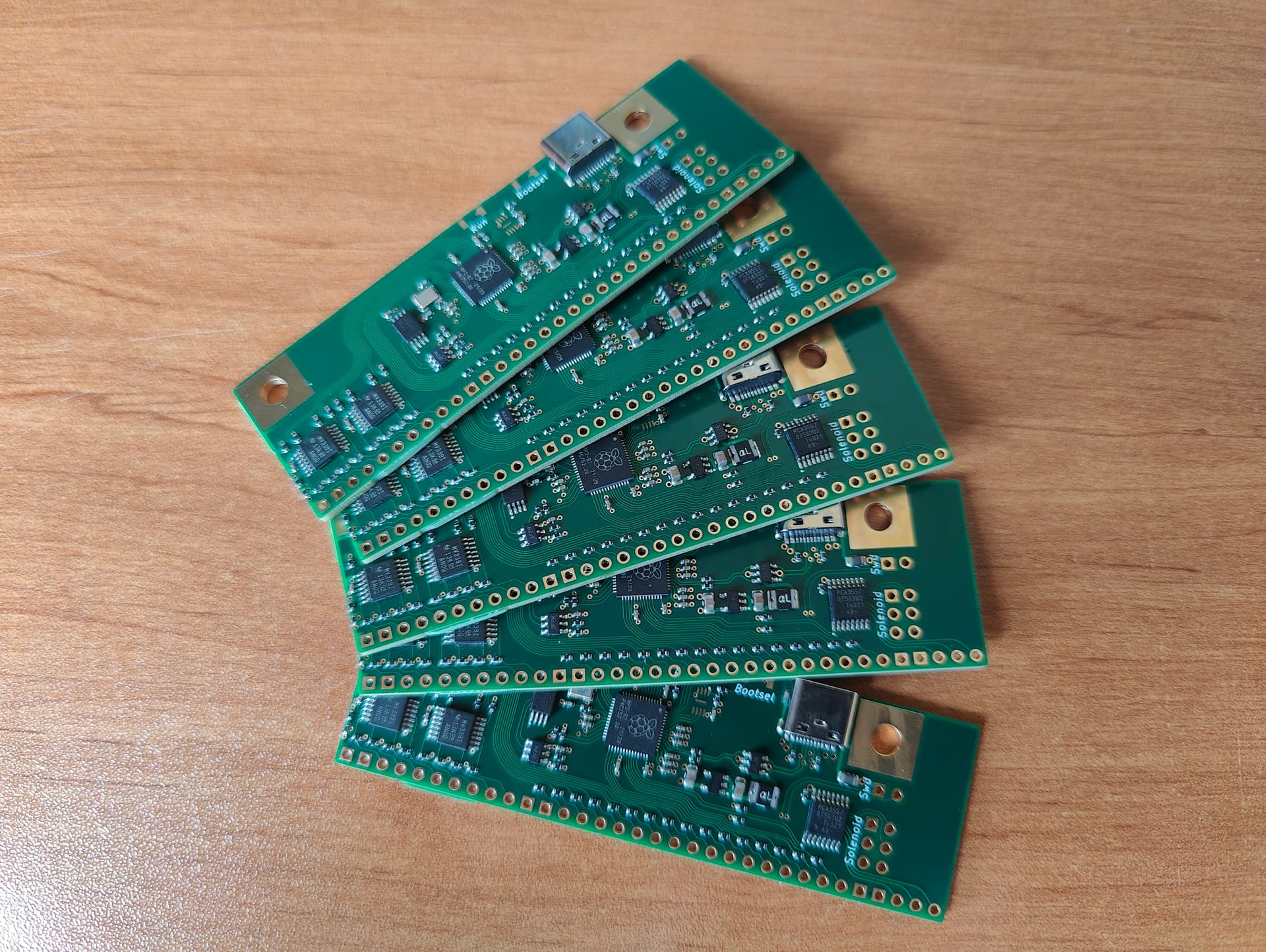
I should be able to order my first fully assembled PCBs at JLCPCB very soon.
Here is a graphic view of the PCB.
Top
Bottom
See ya people!