This is KIL0 => This is my project

Hey there fellow keeb makers,

long time lurker and maker finally putting hands on my diy keyboard project.
My name is Daniel, I’m an electronics development engineer and long time maker from germany (3D-printing, custom electronics, tinkering with some arduinos, …).
I started looking into building a custom keyboard actually for my wife about two years ago because nothing in the market would fit her requirements. I bought two sets of brown Gateron G Pro Switches and ordered five sets of Adafruits neoKey 5x6 ortho snap-apart with two KB2040 to test out different layouts. But like with many projects while these parts were shipped to germany, other projects became bigger priority, but I regularly went back to do some research on all diy keyboards.

So when my second (!) G910 I’m currently using started to experience the same double stroke issues like the first one I had, I picked this project back up, now whit a relatively clear view about the most design choices of the keyboard.

The requirements:

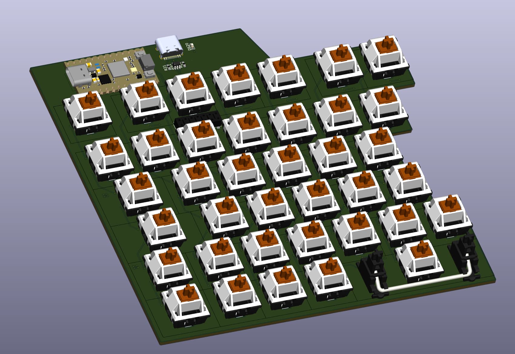
  • 100% design with ISO layout
  • wired
  • snap keyboard
  • highly modular (hot swap)
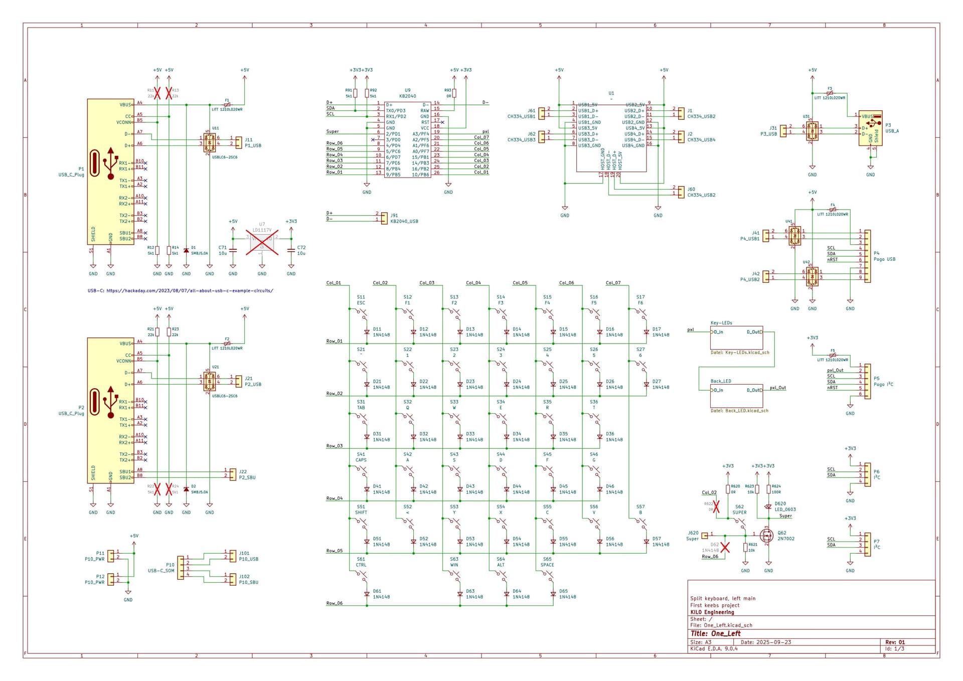
  • KB2040 as MCU

I am kind a nerdo when it comes to making a pcb for my own projects. I usually want to have as many possibilities to use it in different ways as I possibly can cram into it. This is partly due to my professional background as a developer and partly because I’m usually working on projects in segmented time slots and keep forgetting stuff (I am totally lazy in documenting :stuck_out_tongue: ).

The plan:

  • Main Keyboard 60% layout with function keys in split configuration
  • Arrow pad and num pad as snap on modules with own MCUs (I will get into this later)
  • Macro pad and 6 axis space mouse as snap on modules with own MCUs
  • All units usable as stand alone via USB and QMK firmware

The technical aspects:

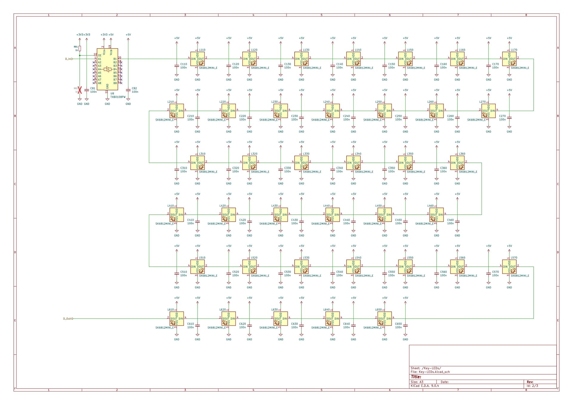
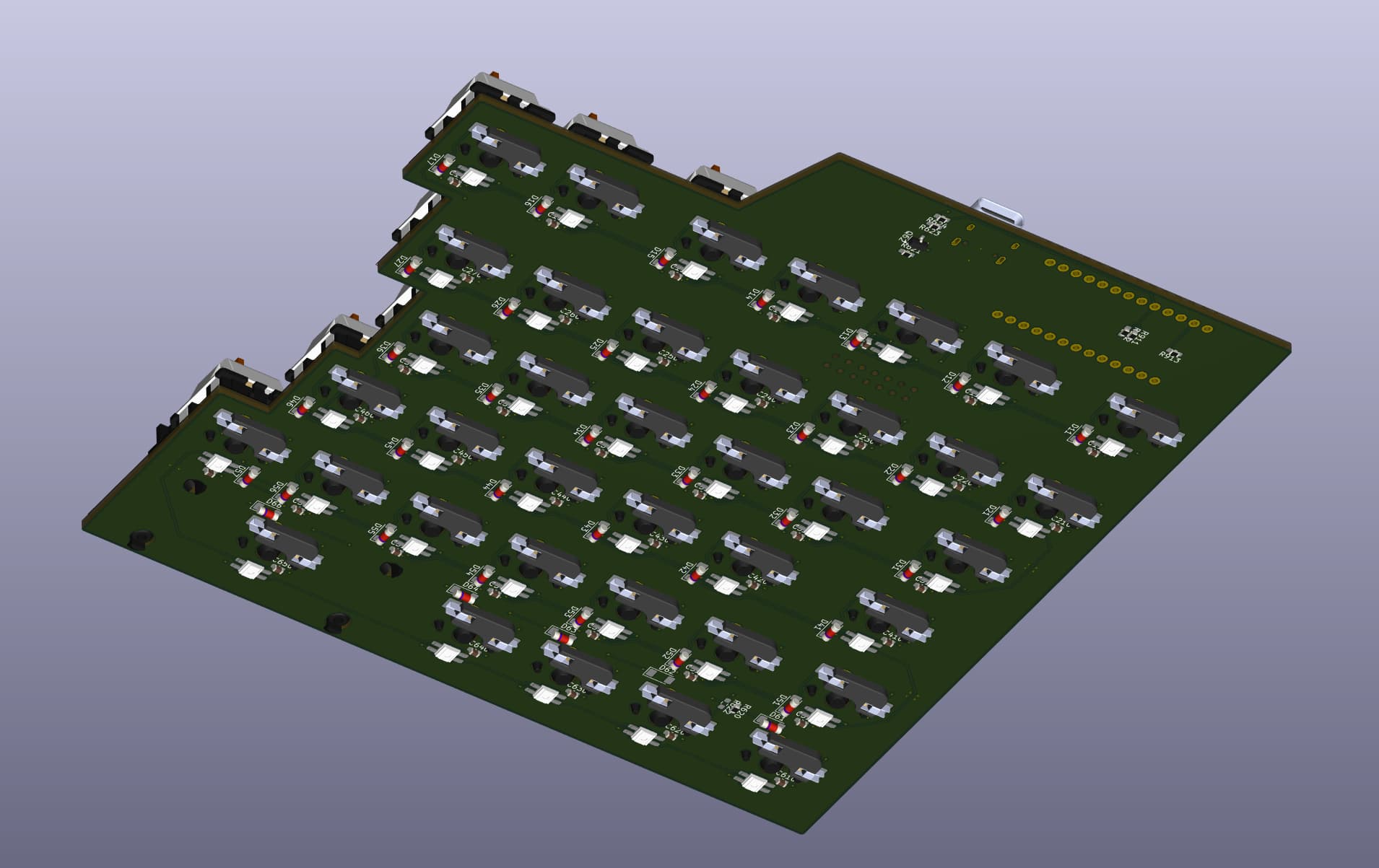
  • Every piece of the keyboard gets it’s own KB2040
  • The left and right main parts are connected with spiral USB-C cable (like UHK 60 v2)
  • The snap on modules can be connected with magnetic pogo connectors to the left and right of the main modules (protocol is discussed later)

I highly like the design of the UHK 60 v2 but it does not fit all the requrements like having function keys ect. What I like are the thumb modules that can be screwed on, to me it looks like they connect via I²C to the main board but due to them being screwed in place I think they can not be hot swopped.

The current idea for the connection between the units via the pogo pins is to use the USB connection. Therefore the USB connection from the MCU can be switched between the USB-C connector on the edge of the board to the pogo pin connector via TS3USB30, activated by Vbus of the USB-C connector (priority, level corrected to the IC).

To handle all the USB communication I plan to implement a CH334 USB hub in the left and right main modules. With this setup I could use USB for the connection of the left and right main keyboard parts as well, handling them as individual USB keyboards all along.

The problem with this is, that I want to syncronize (momentary) layer switching between the two main modules. This is typically done with I²C (if my research is correct) but due to the mapping happening in the keyboard and not in an application on the receiving device (what I highly like) I did not get any results when searching for a solution to this via USB. The alternative to this would be to drop the USB connection between the modules and implement it via I²C. But due to there not beeing a hot swap functionality this means that I need to reset the keyboard every time that I connect a module.

An alternative thought was to use the super speed contact pairs on the cable between the two main modules to indicate the press of a super key for syncronisation.

I would highly appreciate your feedback on my project. I have some more stuff up my sleve when getting into the details but that’s the great picture ,)

Regards

Daniel

8 Likes

Wow, that sounds like a neat project, especially the modularity!

Synchronizing layers via USB is going to be tricky, as the HID protocol is mostly one-way from the device to the host. This is why Via and other dynamic remapping systems use a generic USB ACM interface to control that. Which you could use, but you’d need some software on the host side of the connection to handle synchronization.

I2C isn’t normally hot plug, but I think there might be chips that can do that? But would probably require some bus resetting every hot plug. Is UART or 1-wire an option, maybe?

If you’re using USB-C 3.0+ cables, I want to say there’s some alternate wires for signalling besides the usual 2.0 and 3.0 bus wires, for just this sort of thing (a bit like HDMI has CEC for remote control). That way you can use standard cables and don’t have to worry about it confusing the hell out of an actual USB 3.0 host.

3 Likes

From the engineering side of view there is no restriction for I²C to be hot pluggable, the question would just be how often the I²C master “scanns” the bus for participants. Usually there is nothing on the protocoll level implemented for a client to register itself at the master. And the scanning usually just sends a request and checks if there is a response before a timeout. So this is a litte lime consuming.

I think I will go down the path with the communication over USB and use some of the additional wires of the USB C cables to create something like an interface for the super keys to the other module. Your comment on this sounds like you have a suggestion on which pins to use for this?

I am currently planning to put all the USB and pogo connectors on the main pcb of the keyboard but connect them only to some tht pads. With this configuration the USB connection can be wired with actual wires for each situation.

1 Like

I had some time to set up the first schematic for the left main unit.

Main page contains the key matrix, the SOMs (KB2040 as MCU, CH334 USB hub) and all the connectors:

  • P1 and P2 are USB C ports at the back of the housing
    • P1 is planned for the main connection to my computer => Sink config
    • P2 is held for as input for the right main unit => Source config
  • P10 is planned as USB C port for USB C spiral cable to the right main unit
    • I want the straight piece to disappear inside the housing so I need the connector to be in the middle of the pcb. Therefore I need to lift it up from the main pcb (because otherwise the connector would just not fit)
    • Breakout board will contain the polyfuse, the ESD protection and the source configuration resistors
  • P3 is an old school USB A connector as a spare
  • P4 is dual USB and I²C pogo connector to connect extension modules
  • P5 is I²C pogo connctor for thumb pads
  • P6 and P7 are I²C connectors for displays and other stuff inside the keyboard module

I modified the super key (S62) to have a mosfet driving the MCU pin. The gate pin of the n-fet will be linked thru to the right main module with the same schematic. With this configuration both super keys can be read by both MCUs without rising damaging the MCU.

Picture in the next post

I planned the key lighting and implemented a logic level shifter. For the underglow I designed a footprint for the SK6812SIDE leds. Currently I have “just” 16 pcs for this side, if this number will change depends on the layout and your feedback ,)

Picture in the next post

My plan is to have absolutely no parts on the top of the pcb to be able to clean it very easy (just remove all the connectors and have a clean sweep).

Current thoughts:
As I’m writing this I think I will implement some ESD protecion to the I²C pogo pins as well.

I will try to get to the layout soon. I am intrigued what changes I will/want to do while doing the layout.

Key leds

Underglow leds

I started working on the layout and after placing all the switches and key leds I took some time thinking about the placement of the additional USB connectors and the USB hub.

I revised the plan to put everything onto one pcb and will now be going to make a pcb stack like the nullbits keyboards with the USB connectivity and the underglow leds on the bottom board. It should be possible to design the pcbs in a way that the upper pcb could be used stand alone as a simple keyboard.

About the underglow:

I would be happy about everyone sharing some experiences about the underglow regarding placement, spacing and maybe even the impact of the color of the pcbs (if it has some).

1 Like

Found the place where I read about them – they’re called SB1 and SB2 (SB = side band), but seems like there is some negotiation you have to do over the CC1/2 lines to use them (vs fixed resistors). But also seems that you can use that same negotiation process to use the high speed wires for alternate uses, as well.

Good luck! If you’re using the reverse-mount ones, I’d suggest quadruple checking your footprint and maybe even getting a small test board made to verify it. I managed to screw up the footprint for these not once, not twice, but three freaking times. Once reversed, once mirrored/rotated and I forget the last one. (I did finally get it working, though!)

Off the top of my head:

  • If you are using serial RGB LEDs (WS2811’s, SK6812’s, or similar) and planning on both underglow and per-key LEDs, put them in one single chain rather than have two different pins.
    • This is because it’s a PITA to get QMK to do RGB on two separate channels (it wants ONE driver configured for rgb matrix, and while you can have rgblight and matrix going at once, you wind up having to write a custom bit-bang driver for one of them because the usual ones conflict)
    • With a single chain, you just use rgb matrix and set bitflags for which ones are per-key and which ones are underglow.
  • Placement: try to evenly space them. edges first as that’s the part that is more likely to be visible. Though it really heavily depends on the case and it’s transparency. Note that you’ll want to make sure the QMK configuration matches the placement on the PCB so the effects look correct. I’ve seen a lot of boards that assume ortholinear RGB positioning on a standard staggered layout and it shows.
  • For PCB color, it doesn’t matter too much: I went with white to maximize reflections and thus brightness, but I’ve not noticed a big difference between dark PCBs vs. light.
  • Watch your power usage with RGB. I loaded up a 60% with per-key and underglow and only doing half-brightness I was pulling nearly 1.5A, waaaaay outside the max 500mA I was supposed to be drawing.

Thanks a lot for your thoughts!

I loaded the lib provided by Joe Scotto and checked the footprint against data sheet and 3D and it does match. The 3D functionalities of KiCad is one of the many things that make this ECAD so much more potent than other free ECADs out there.

The thing with the additional data lines on the USB-C is clear to me, thing is that I need to check out how the port behaves on side of a computer (or other end device) that really supports all functionality the USB-C brings with it for high speed if there is communication just on USB 2 protocol (D+/-) and one pin toggling between 3V3 and 0V.
To keep the end device out for good there is still the possibility to connect the keyboard with a USB-C to USB-A cable where these data lines simply just don’t exist. The connections between the keyboard modules is uncritical because I am in control of both sided of the cable. But for good I want to check out how end devices would behave. I will get myself an Adafruit 4090 breakout board just to measure how the not used ports behave.

I took some thought yesterday again while talking to a friend of mine (also electronics dev) about this topic and I found a USB-C spiral cable with angled connectors on both sides that I ordered for connecting the two main modules. With this cable I get around having an additional USB C in the middle of the module that creates a lot of space and routing issues.
I will create two USB C connectors above each other, one on the top pcb (USB input for USB hub) and one on the bottom pcb (USB to host). With this solution I can route all USB directly without having solder pads of jumpers for the routing. To minimize the height of the stack I will implement the CH334 in form of the CH334U in QSOP-28 package directly on the bottom pcb. The pogo connectors will also move to the bottom board.

For the underglow I want to use SK6812SIDE-A leds in serial to the key leds. I was looking for placement references when I stumbled about this video using the exact same leds (or at least the build factor).
Moving the underglow to the bottom pcb enables me to have enough space to place them with a constant distance to the edge of the board without having any obstacles to worry about and stay far enough away from the board edge to create a homogenous glow.

For connecting the top and bottom board I will get connectors like the Samtec HLE-110-02-L-DV. There are cheaper variants available on LCSC that are a bit higher (5mm compared to the 3.66mm of the Samtec), they will do de job just fine.
I also ordered some solder in threaded sockets with 4,5mm height above the board, so the distance between the bottom and top board will be around 4,5 to 5,0mm. This gives me enough pace to have 2mm heigh parts on both pcbs without to worry about collisions.

For diffusing the underglow and closing up the space between the pcbs I will use a 3d printed frame made with clear petg for the first model.

1 Like

I thought about current consumption too, especially because I have all devices powered over one usb port.

The lighting won’t be full circus, I usually just want to being able to see the keys when having the light out at night (real basement kid. I also have 5050 rgb strips embedded in my desk and behind my screens for indirect lighing, I want to connect these to openRGB as well but I have not found a real solution how to do this.

For my desk I thought about using a USB power injector like this. But I want to have a model for my desk at work too but there I will just disable the lighting.

Your comment on pcb color is very good to know. I will then purchase the pcbs in black to keep it simple.

2 Likes

I went ahead with the layout of the top pcb:

I am going to start with the bottom pcb next, maybe until then I get some feedback from you about the following questions:

  • What supply voltage is typically used within the community? Data sheet does not specify 3.3V supply but with 5V supply 3,3V high level would not be sufficient. I’ve seen a discussion of some people using diodes to alter the supply voltage and some people using 3V3 supply but mentioning that it could effect the blue led maximum output
  • I am thinking about adding two headers to the top row for mounting a pcb with additional keys above the MCU. On my G910 I have some smaller switches (M1, M2, M3, MR) to controll the macros. They feel like smaller versions of the other keyswitches. Does anyone know what switches these could be?
  • What is the community “standard” regarding pcb prints?

Hey there,
I have a quick update on my quest for this keyboard system:

I did some more research, looked into some modules for validation/verification of my plans/ideas and ordered some. I also stumbled over a corne v3 set for good price @ pandakb and ordered it.
The corne is completely on the other side of the keyboard spectrum but it was quite cheap to get (40€ incl. shipping, only missing switches [that I already have laying around] and case [3dprint]).

What I find quite interesting about the QMK version of the corne v3 is that it does not mind on which of the two halves the USB connection to the PC is established. Also there is a trackpoint module available from holykeebs that I absolutely will get. I used the trackpoint on my T430 extensively during my studies and I still use it at work when being aroud with the laptop rather than carying a mouse with me so I will give this a go for the corne.

I also reviewed this video where the creator achieved something like a hot swap I²C infrastructure.
I don’t want to change from the concept of the integrated USB hub and connectivity of each device, but f.e. for the thumb pads I would rather use I²C than usb due to them beeing quite useless stand alone and it solves some space issues.

I also ordered an MCP23017 IO expander break out to have a little fun with qmk and this just to get a feeling for what could be done.

1 Like