Hello everyone! Thanks for stopping by this post. Hope you are having a great day 
Before we jump into the keyboard, a bit of background:
- This is a personal learning project. I’m a complete newbie to keyboard design (and basic electrical engineering principles). If I look like I don’t know what I’m doing, that is because I don’t know what I’m doing…
- The purpose of this post is to document my journey into keyboard design as well as share lessons learned along the way. So any feedback and advice will be greatly appreciated!
- I was heavily inspired by a lot of excellent members in this community, especially @Rico. Also, for anyone who starts as green as I am, I highly recommend the 5-episode series by Mr. Keebs and Gondolindrium on YouTube when they streamed making a PCB from scratch.
All right, with those out of the way, let’s get to the board:
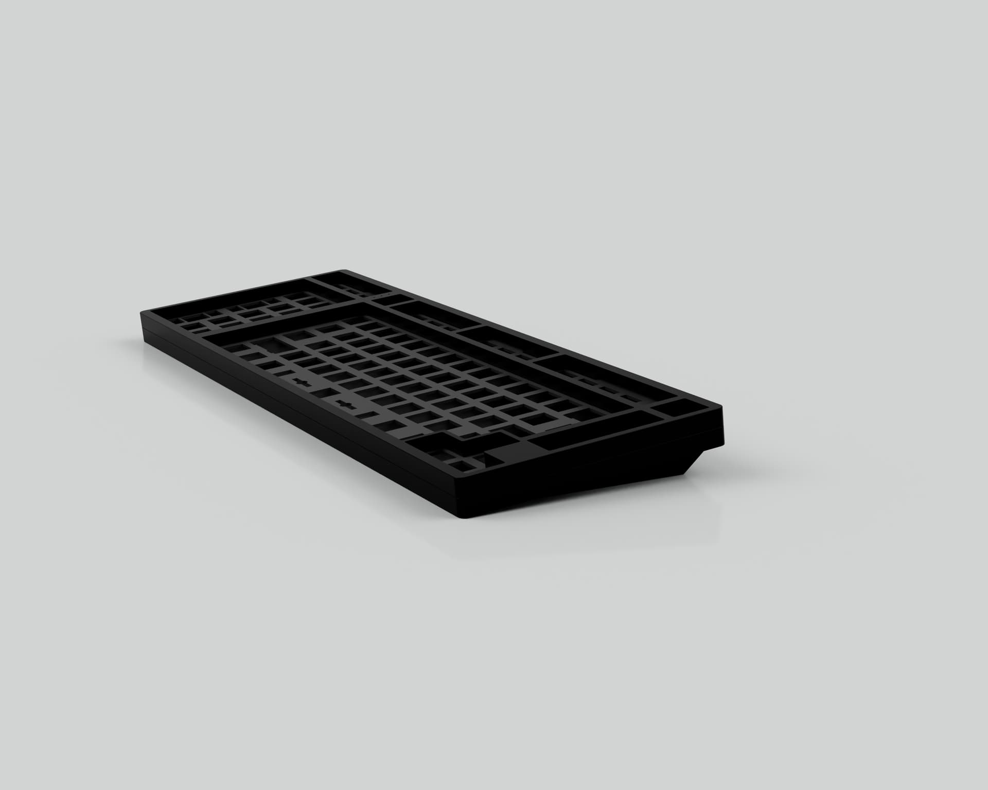
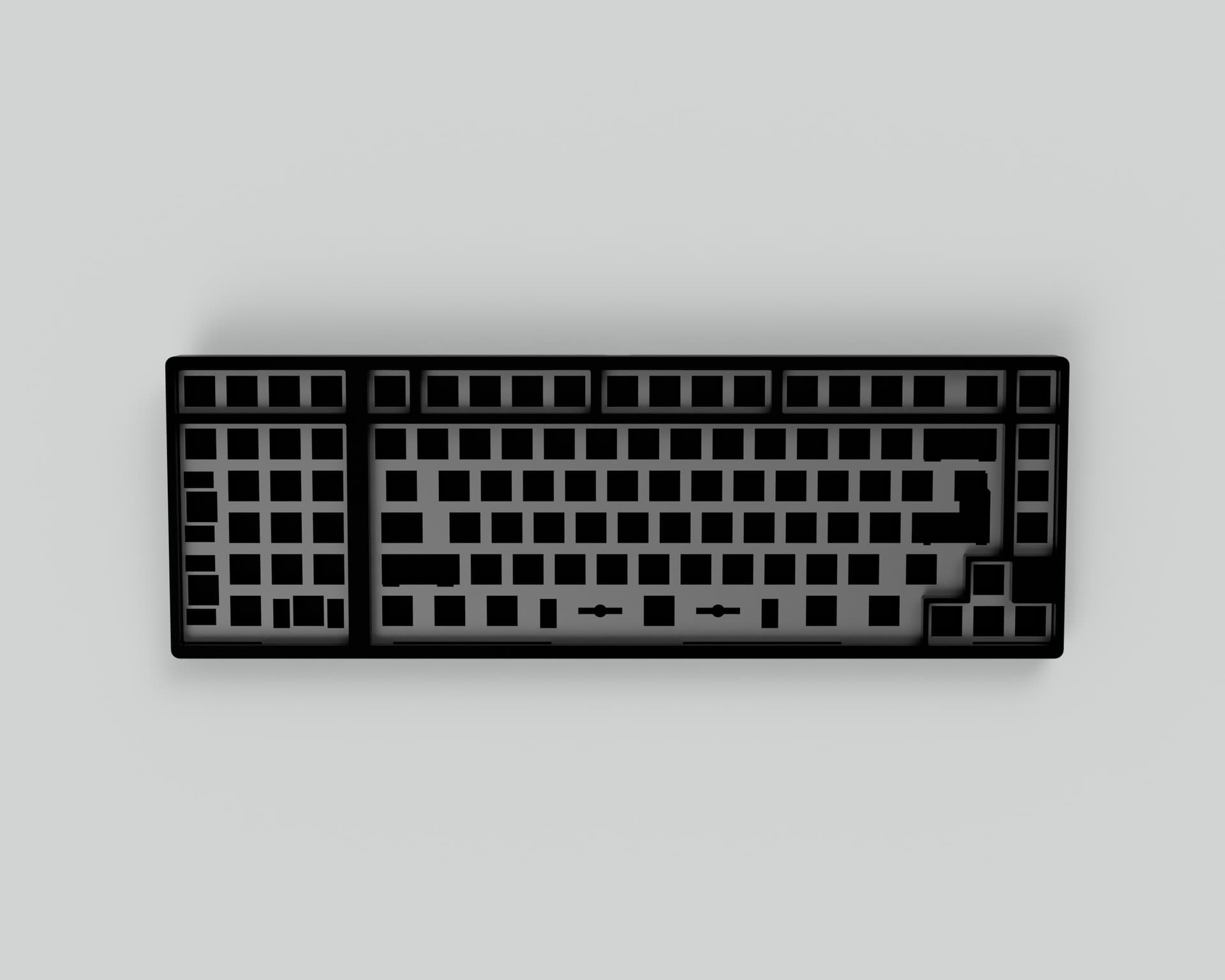
Key Features
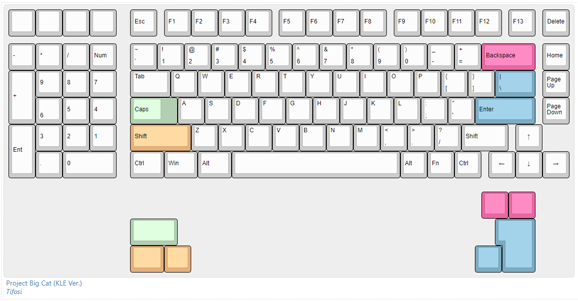
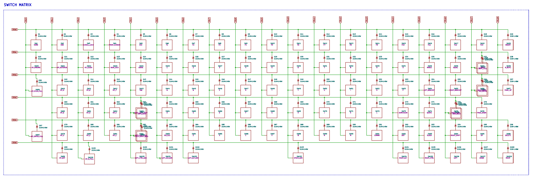
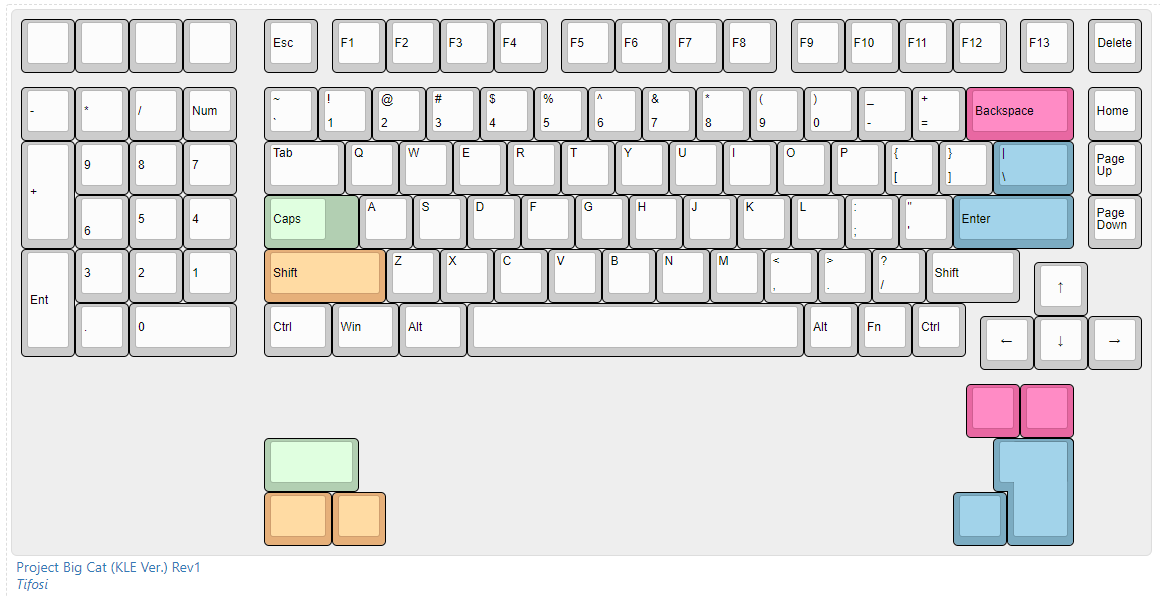
- Semi-compact 1800 southpaw
- Hotswap with some ISO layout support (for learning purposes)
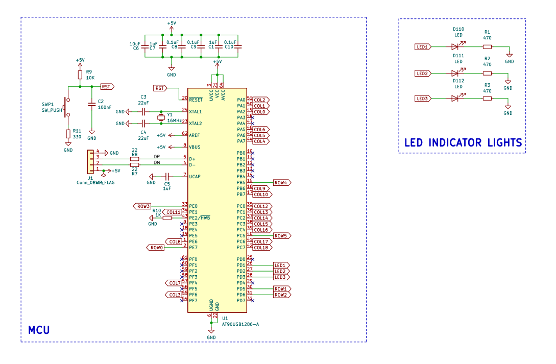
- Utilizes Ai03 unified daughterboard
- LED indicator lights for Caps, Num, and Scroll Lock
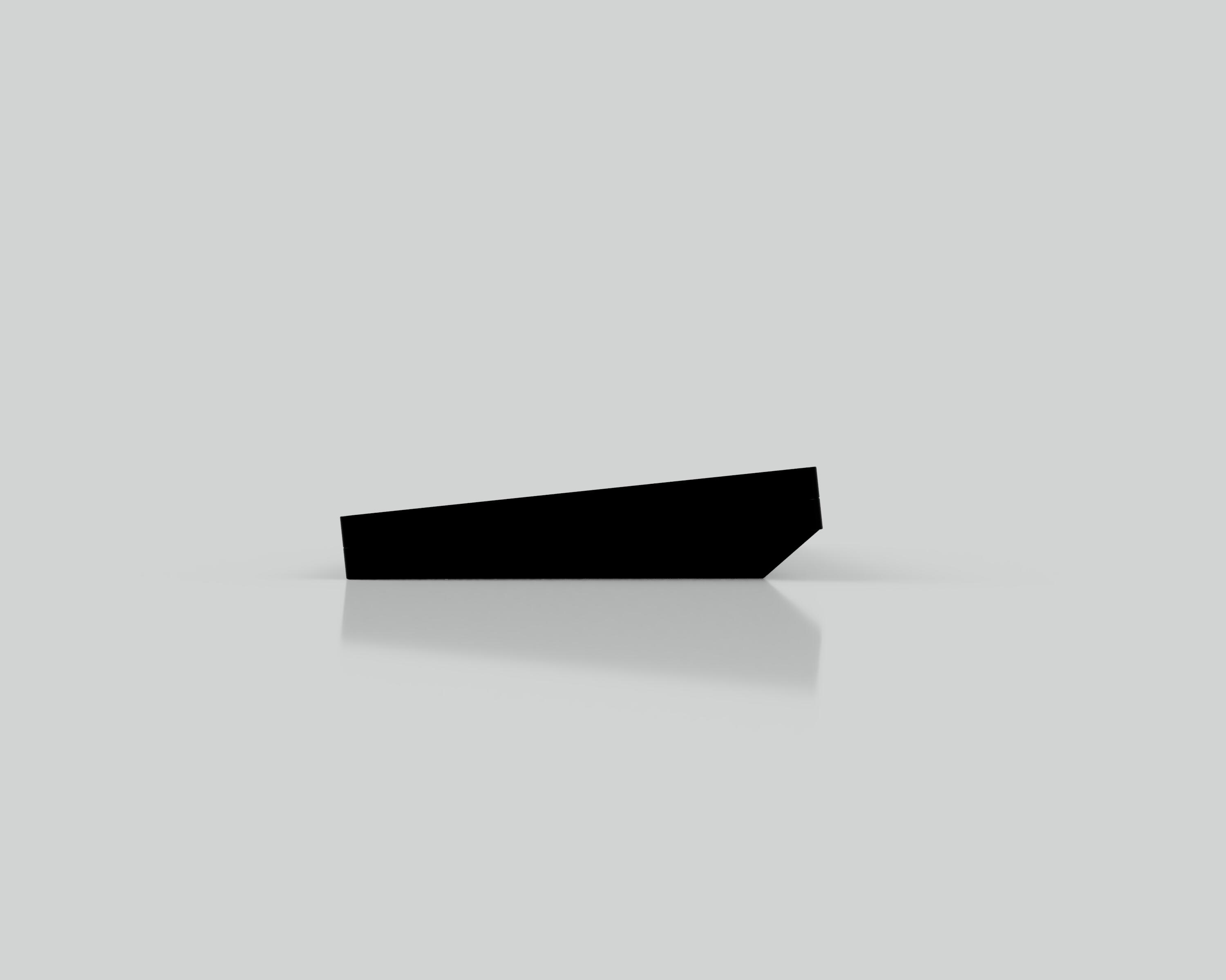
- Aluminum case (top mounted or gasket mounted, tbd)
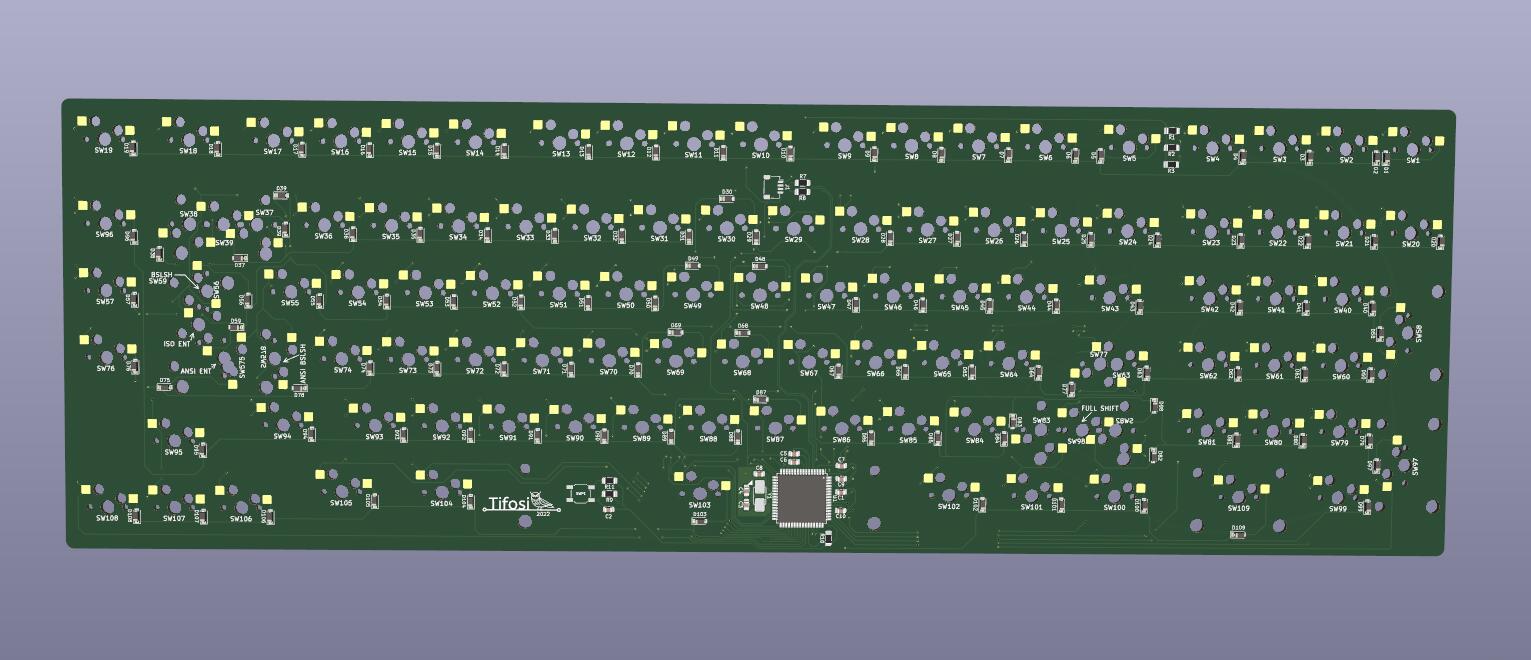
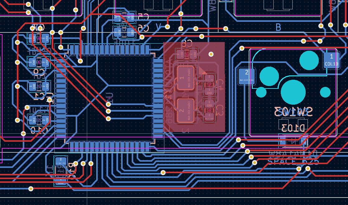
PCB Schematics
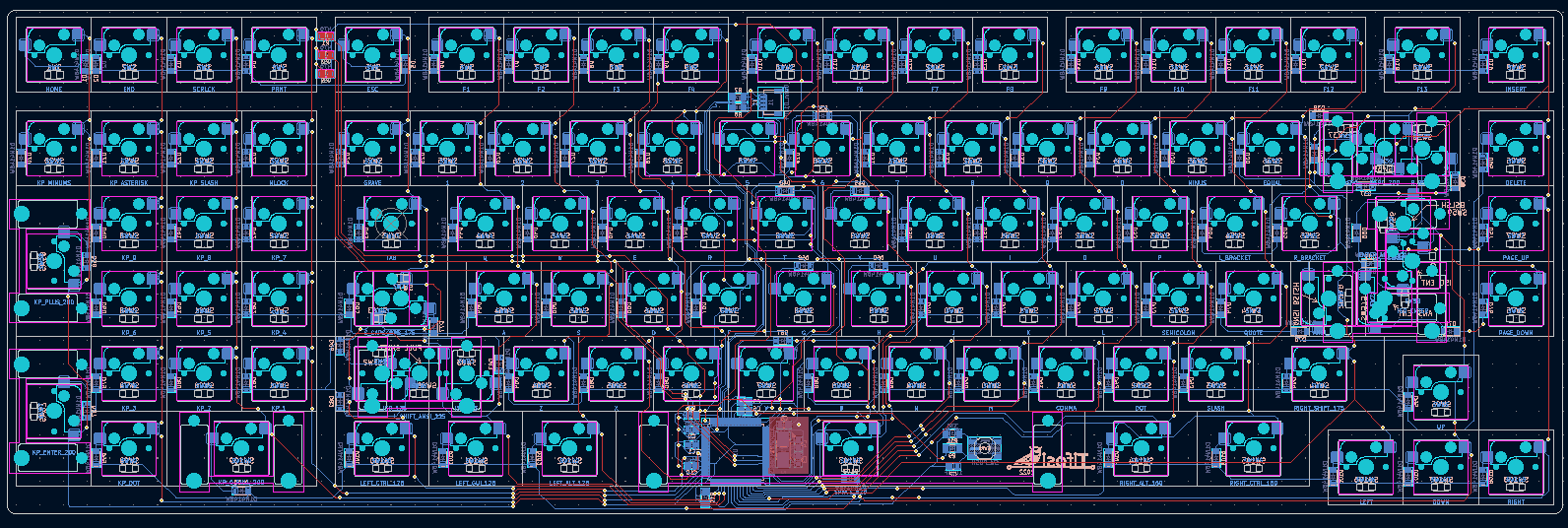
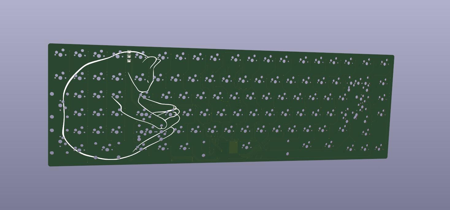
PCB in KiCAD
Questions still needs to be resolved
- Ground Planes and Ground Pours: I only have two ground planes (front and back) surrounding the crystal. Is this sufficient? I’ve seen people making ground pours on front and back, but I’ve also seen that this might not be necessary for a two-layer PCB?
- Routing: I know that I’m supposed to keep stuff away from the differential pair and the crystal, but real estate is at a premium. Am I keeping enough clearance?
- Any other glaring issues that a newbie just wouldn’t see?
Next Steps
- Order PCB and components
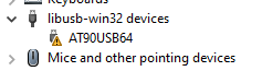
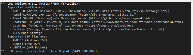
- Learn to compile firmware in QMK
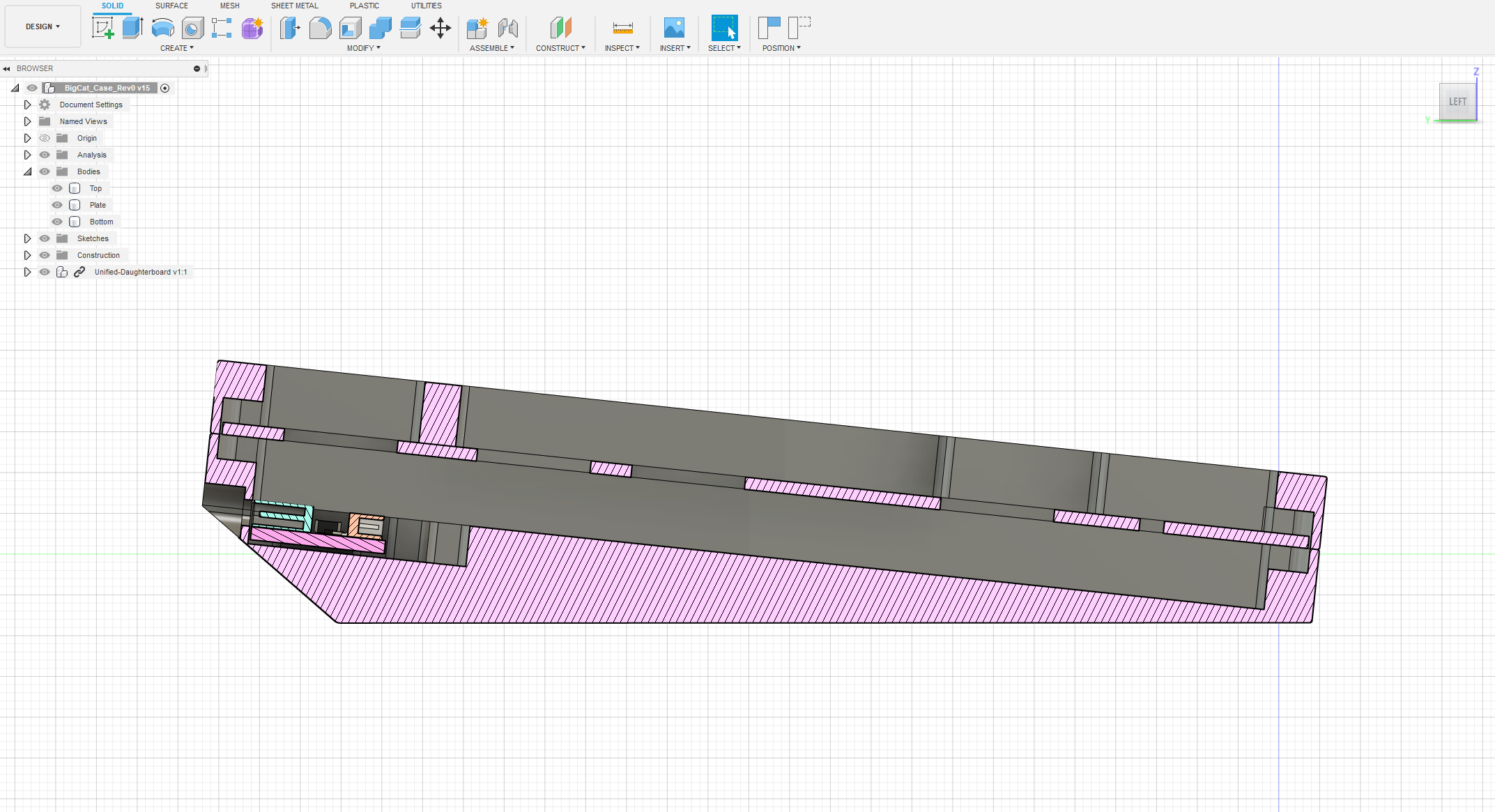
- Learn to design case in Fusion 360
If you are still with me at this point, thank you for your patience! I will be back with another update (hopefully) soon…


 Thank you so much for your advice and encouragement!! I will adjust those routings as you suggested
 Time to go shop at Digi-Key again
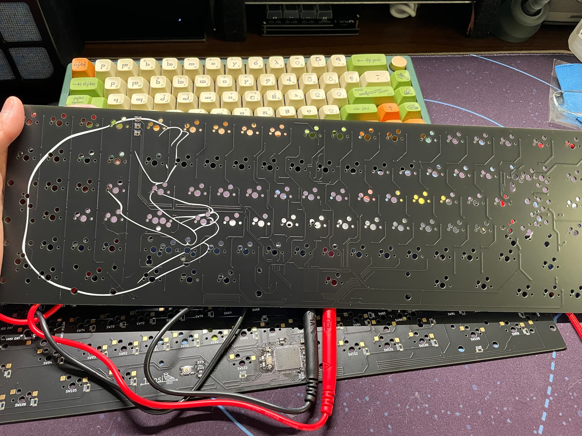
 Life got super busy last week, but I’m back with some quick late night updates: