The Manta75 - A new keyboard design from the Sea Collection - now an opensource project!

Hello keeb lovers,

My previous project, the Winghead, finished months ago and I really enjoyed the design and craft work implied.
The end result was not perfect but a significative improvement over my first attempt, the Simply96, and I enjoy using it everyday at home or at work (so is the case for my brother who has one).

Roughly one year has passed since this project began at it is now time for me to start another one!
I try as much as possible for my keyboard frivolities to at least benefit my close family, this time is no different.
My two daughters turned 15 this summer and will soon each need a computer for their homework.
So why not also offer them a special keyboard to go with ?

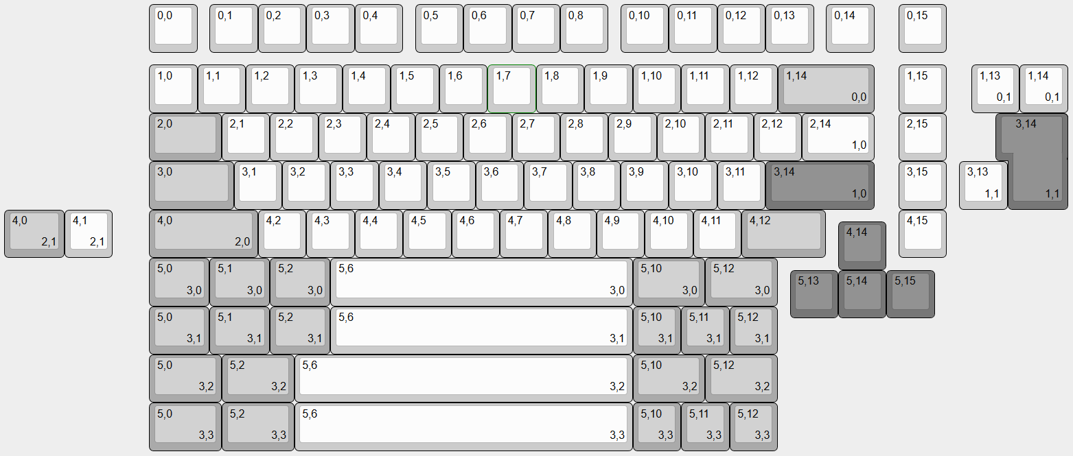
After discussing their needs and the layouts they’d want we decided on a 75% like layout.
The Manta75 project was born.

The name comes from the ‘manta ray’, a big and majestuous fish that you can find in the Pacific ocean.
This keyboard will be second of the ‘Sea Collection’ (the Winghead was the first), trying to find inspiration from the marine species.

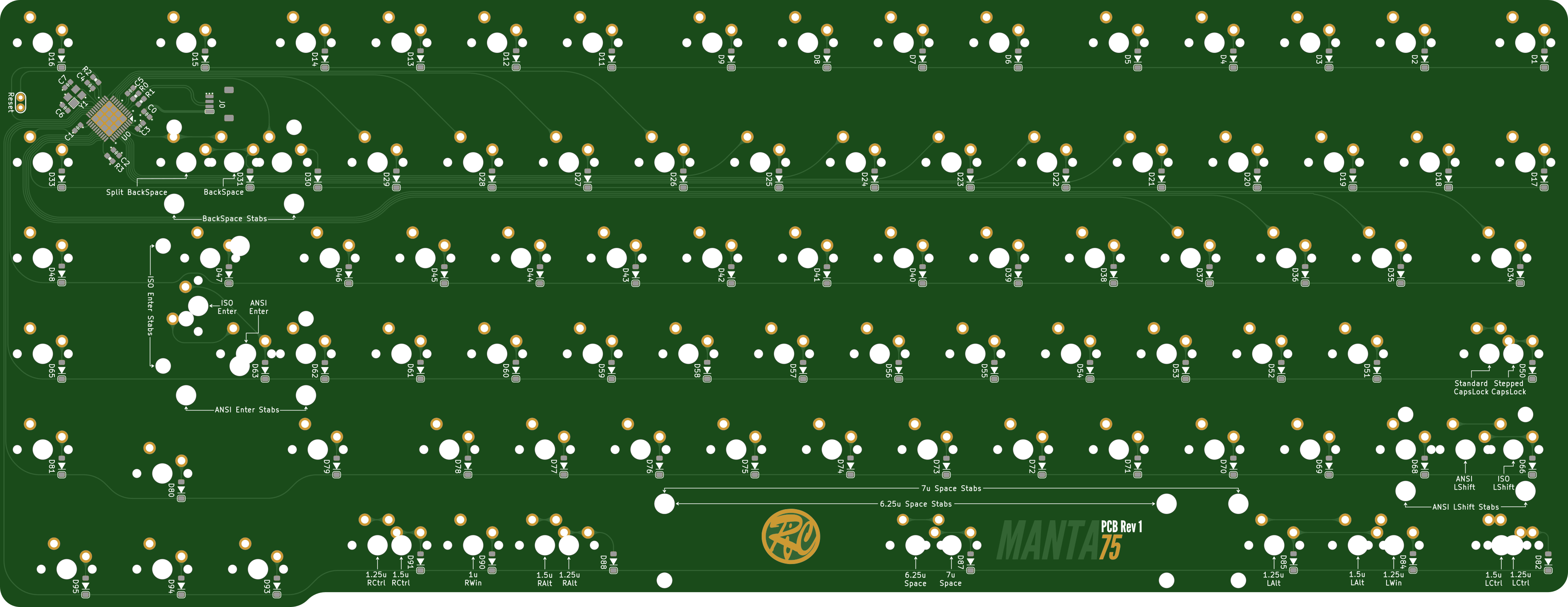
The first work was to define the layouts using KLE.
I wanted to physically separate the different key groups, and most importantly the arrow keys.
I did liked the Satifaction75 layout and took inspiration from it but not the knob so a simple key is replacing it, a nice place to put an artisan for example.

Here is what I came to:

Now onto the goals in mind.

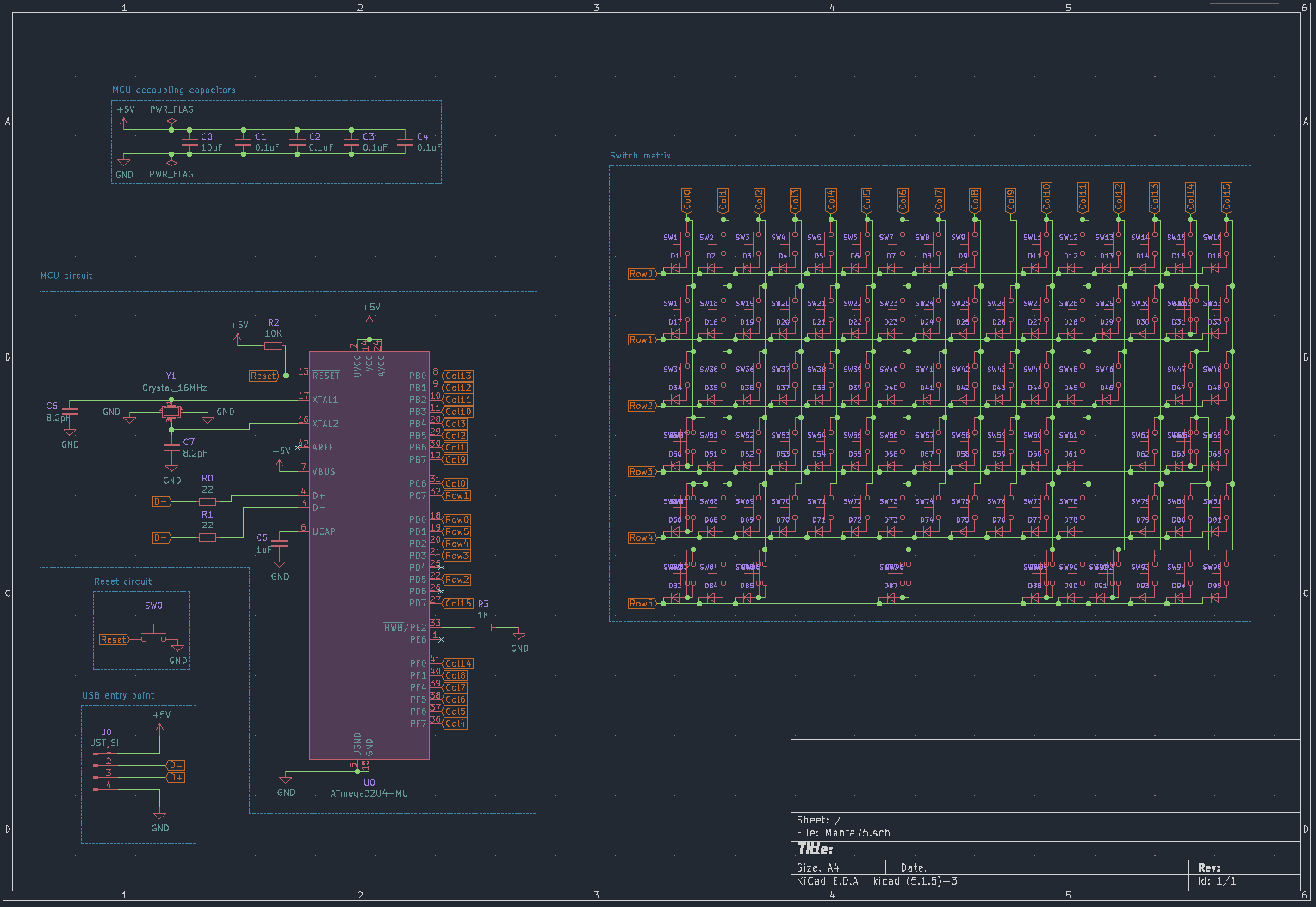
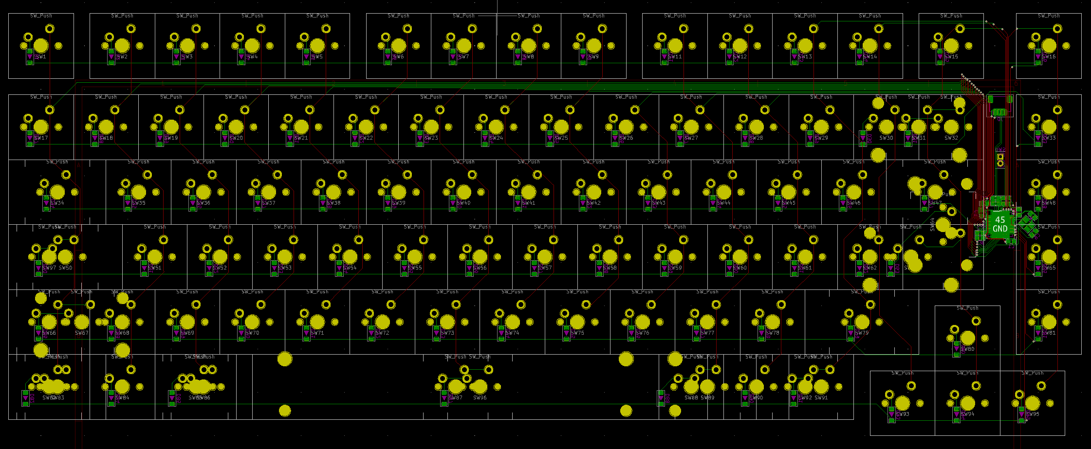
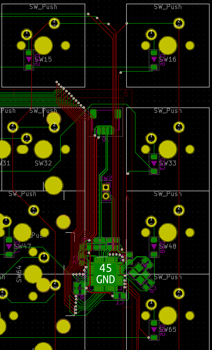
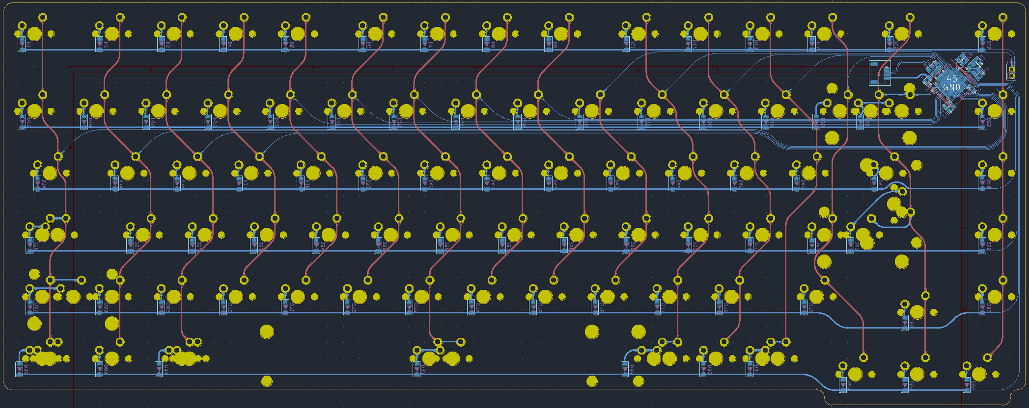
The PCB design (already started)

Functionnality will be as basic as a keyboard can be:

  • QMK and VIA compatible
  • No leds.
  • ANSI and ISO compatible.

My previous PCB design focused on reliability and not on look.
This time I’d like to push myself more on making a nice PCB, having the minimum of functions on the board (the reason of no leds) will ease this task.
Let’s make a good looking PCB this time!

The case

The design has not started yet but would like to keep and improve on what worked great on the Winghead:

  • Limited void space between PCB and bottom case, is 3mm on the Winghead.
  • Sandwitch mount.
  • Leaf spring design.
  • As low profile as possible for a high profile, front height is 18mm for the Winghead with bumpons.
  • A reasonable slope, Winhead is 5 degree and may like to increase it a bit, 6.5 degree to an absolute max.

To my mind the biggest success of the Winghead is it’s sound signature.
There is no hollowness and no metal ping, the sound is a nice ‘thick’ with GMK caps, and more ‘thock’ with higher caps like MT3.
This is also quite a silent board even wihout silent switches, probably the most silent board at my work office (were MX browns reign supreme).
I really want to duplicate this result on the Manta75 this is why I intend to keep most of its features.

See you :slight_smile:

8 Likes

Sounds nice. Looking forward to seeing the case design now.

1 Like

Sounds like something I want one of. :+1:

1 Like

This will take quite some time, be patient :wink:

I got all the time. Don’t worry. I’ll enjoy seeing it whenever it comes up. A good design is worth the time. :wink:

1 Like

Me to wants to give my daughter a keyboard. She’s only 4 years old (soon 5) so I’m in no hurry.
My plan is to build her a pink-themed keeb so I will probably get Bliss r2 so it might be done by the time she turns 6 years. :tada:

3 Likes

Looks interesting, you’ve peaked my interest

2 Likes

Haha!

1 Like

Imagine having a dad as a 15yr old that creates you you’re own custom keyboard.
Nah, but specs sound nice, like the layout and looking forward to case design.

1 Like

Awesome! Happy to see you diving in again, your design threads are must-reads for me.

1 Like

Hello keeb fans!

As told previously I wanted to focus more on making a good looking PCB.

  1. But what is a good looking PCB design?
  2. And most importantly what is a good PCB design overall?

To answer the question 2 (opinions may differ, fell free to comment), a good keyboard PCB design should be one that works reliably without any aestetics considerations.
It implies engineering care of the most critical parts of a keyboard PCB design, including:

  • Care to make a good USB differential pairs routing.
  • Decoupling capacitors placed near MCU.
  • Crystal near the MCU with correct load capacitors values (if you use one like with ATMega MCUs).

A keyboard PCB design is surprisingly easy electronically and looks quite forgiving: even if all these rules are not correctly applied you’d be surprised to see a design still working in practice (with more or less stability issues).

And for question 1 a good looking PCB should be one that takes care of having harmonious trace routing, with consideration of global PCB aestetics.
Adding custom graphics and logos is often a welcomed addition to add aestetic value.
Wilba PCBs are just georgous to say the least.
So are Gondolindrim designs with the bonus of being open source, higly recommend to look at it’s designs here: Acheron Project · GitHub

So 2 is the most important factor but adding 1 would be cool.

Can’t tell myself if my designs are good (or good enough), at least I did my best to follow these basic rules and so far didn’t see any stability problems, fingers crossed :stuck_out_tongue:
Being concentrated on reliability and not look (until now), one thing is sure is that they are not looking nice :smiley:
So let’s try to change that for this design!

Before launching Kicad and go crazy on designing I had something important to do, that is create a KLE layout for VIA.
Doing that allows to visually see row/column patterns of your layout and it is very handy to create a good switch matrix layout in Kicad schematic editor.
I did not do that for the Winghead and I inevitably ended with a mess of traces when routing the PCB, it was time to learn from my mistakes and improve the process.
Here it is:

Schematic was quickly finished, being based on an ATMega32u4 that I already used before in the Winghead:

And at last the PCB routing.

First to do MX switch placement on the PCB.
Did saw all the great videos done by @hadi and recommend having a look at them if you are doing or planning to do keyboard PCB designs:

Had already learned most of its tricks the hard way, by messing with my own designs :smiley:
But he teached me a stupidly simple thing that I never thought by myself: create a user grid were values are based on MX switches units.
MX switches spacing is 19.05 mm or 0.75 inches, took 0.75/8 inches as user grid value (that is 93.75 mils).
This way placing switches on the PCB is super easy and fast.
By bad, was using calculation for placement of each switches before, haha !
So thank you @hadi, you made my life much easier!

Then placing diodes followed by routing switches columns and rows only.
Once done you should clearly see if something is wrong with the switch matrix, and do the correction in the schematic editor if necessary.

Last placing all remaining components and wiring everything.
Did the first try using my usual approximative routing method and came quickly with the folowing result:


So:

  • USB data lines routed with no vias, no crossing traces, and a ground plave below.
  • Decoupling capacitors close to MCU.
  • Crystal with it’s load capacitors well placed close to MCU as well.
  • DRC checks passed.

It will definitively work but it’s not what I call pretty :frowning:
Ideally wanted only column traces visible on the top layer but also have weird looking vertical segments visible for switch matrix and 5V routing (because MCUs often have 5V pins all around their sides).

  1. For switch matrix traces the solution is to better place MCU and components on the PCB.

  2. For 5V routing Gondolindrim does a very neat strick to its designs: a square 5V fill zone on the top layer, just surrounding the MCU and its pins.
    This way you feed your MCU with 5V only with vias on this fill zone, no more ugly traces!

I restarted the PCB routing from scratch using 1 and 2 and came with something much more acceptable.
As I wanted a more organic look of the traces I used later several Kicad plugins to make curved traces and add teardrops to pads.
After a long effort I came with that on Kicad:

I will probably continue to pimp it in the future but it is already much better :wink:

See you!

6 Likes

Thanks for the kind words, Rico! Glad you found the series helpful.

3 Likes

That looks great, but the traces look very dense. What’s their width?

1 Like

Yes, the row and column traces are 20 mils while the others are 8 mils.
To be honest I am also not sure if it is a good decision and may revert to 8 mils for all traces.

Currently looking to design my own PCB and would like to curve the traces on my board. Which KiCad Plugins did you use to curve your traces? They look stellar.

Hello @Suavity!

Here is the github link to the plugin I used for the rounded tracks:

And also the other link to the teardrop plugin:

Beware that rounding tracks is quite a long and tedious process, you will do/undo your work quite some time before having something that is good.
I strongly suggest as a first step to perfectly route all your tracks with the standard 45° angle that Kicad propose; then you can curve these tracks by iteratively testing different radiuses until the good one is found.

Good luck :wink:

2 Likes

Hello everyone and Happy New Year!

Just a little bit of news.
Things have progressed slowly, not as fast as I wanted it to be.
Didn’t made my mind yet on the case design, and plate design is under research stage at the moment.
But I had good progress for the PCB :slight_smile:

One goal for the PCB design was to have something nicer to look at, and think I’ve achieved this.
Nothing crazy of course, but much better than what I did before.
Compared to the early revision I showed in Kicad I did a few tweaks:

  • @deshipu was finding some of the traces too fat, all traces are now at a thinner 8 mils thickness.
  • Some bad switch footprints placement for the botton row have been fixed.
  • Added proper infornation on the silkscreen about switches positions for different layout options. This is something that Gondolindrim does on it’s PCBs and limits the potential mistakes when soldering the switches.
  • Added cool Manta75 and Rico logos :stuck_out_tongue:
  • Revised all component footprints with better and more readable silkscreen information: diodes, capacitors, resistors, MCU, crystal, JST connector.
  • Modified MX switch footprints to be able to use millmax sockets.
  • Tweaked a few traces here and there…

Here is the result:

Another goal of mine was this time to use an SMD assembly service.
JLCPCB is offering one with some limitations to take care of:

  • pretty much limited to green solder mask (black and blue are possible but there are additional constraints, like no ENIG, or no lead free HASL, or minimun order quantity of 30 PCBs, …).
  • limited availabily of components (although they are making progress).
  • one side assembly only.
  • no SMT component assembly.
  • basic components are very cheap and cost pennies to assemble.
  • for each extended component type you have to pay a fee (a few dollars) so care to limit those is important.

Most of these constraints are not a big problem and can be worked around.
And for the color I like green, no big deal.
I could select mostly basic components, with the exception of the ATMEGA32U4 MCU.
Only one component is missing for the assembly, the JST connector that I will solder by hand.

Some may remember that for the Winghead keyboard I could not manage to use their assembly service.
Well this time it went rather smoothly, I had only to modify by hand in the centroid file the rotation of the diodes (they were inverted in the preview) and voilà!
And I could also leaved the centroid file as is: JLCPCB does a manual inspection of all the boards and could have done this work by themselves, but I like when things are perfect :stuck_out_tongue:
JCPCB looked to have improved their workflow, or I improved my PCB design skills, or most probably a bit of both :smiley:

The order is sent, now waiting.

Also ordered a few more components , both at LCSC and Farnell.
For Farnell this is an ESD protection chip of Texas Instrument, used by AI03 universal C3 USB daughter board. This chip is out of stock everywere(LCSC, Digikey, Mouser), only Farnell had 39 remaining. Probably due to the Covid 19 situation :frowning:

So yes, Manta75 uses the great and latest iteration of AI03 USB daughter board C3 design :slight_smile:
Also ordered a bunch of these PCBs (white color solder mask this time).
I will be able to make up to 30 USB daughter boards, I went a bit overboard this time, haha !

See you all, and take care.

3 Likes

This looks really great, you can tell you spent a lot of time on it.
I was actually worried the traces are too thin. Even if the manufacturing spec allows it, I like to keep some margin and only use the thinnest traces where absolutely needed.

2 Likes

Thank you @deshipu!

The traces are 8 mils wide.
Most manufacturers state 6 mils for their minimum specs so there is a bit of margin here :wink:
Also did manufactured a PCB with 6 mils traces a long time ago (using JLCPCB) and it came out great, so I think that with their minimum specs PCB manufacturers already include a margin.

1 Like

Usually you would want to do thicker traces for your power delivery, you can use something like this to calculate the trace width you need, that being said I doubt the keyboard is going to pull more than like 100mA in which case even with 1oz copper 8 mil should be fine.

3 Likes