A couple of months ago I started working on a custom split keyboard. It all really started because my hands are too small for the Ergodox EZ, the crkbd is awesome but doesn’t have enough flash to hold a fully loaded QMK setup and most split keyboards have a noticeable lag when typing very fast.
I have a working prototype now and since there are not many resources available on how to build split keyboards I wanted to share my experience and approach. But first, some specs and images:
Most noteworthy is that the Ganymede keyboard
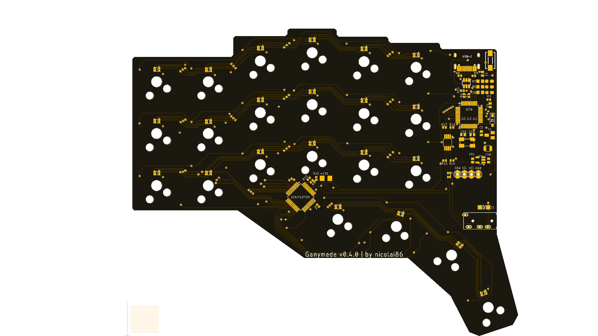
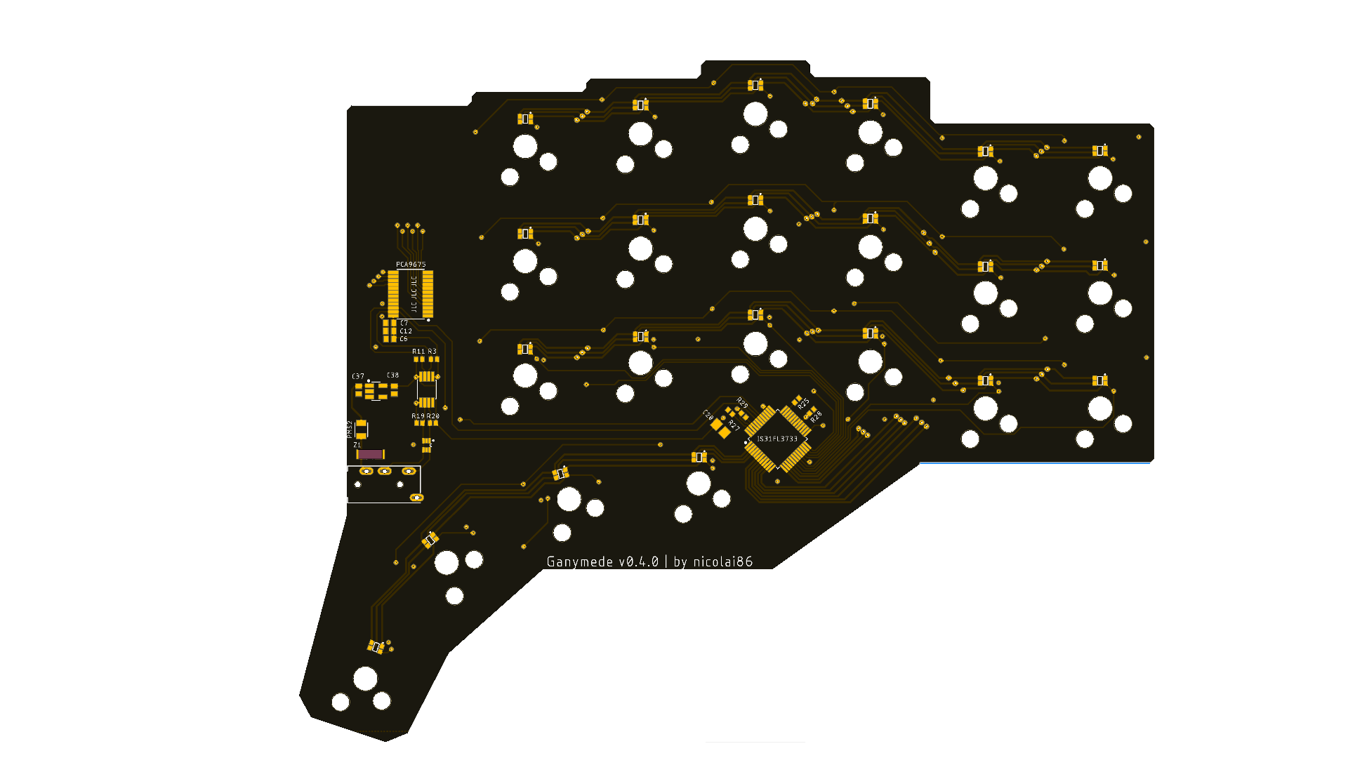
- has a flippable PCB
- uses a STM32F303CCT6 (same as the Proton-C)
- communicates via I2C at 1Mhz between the sides
- has OLED support using I2C2 one the left side and I2C1 on the right side
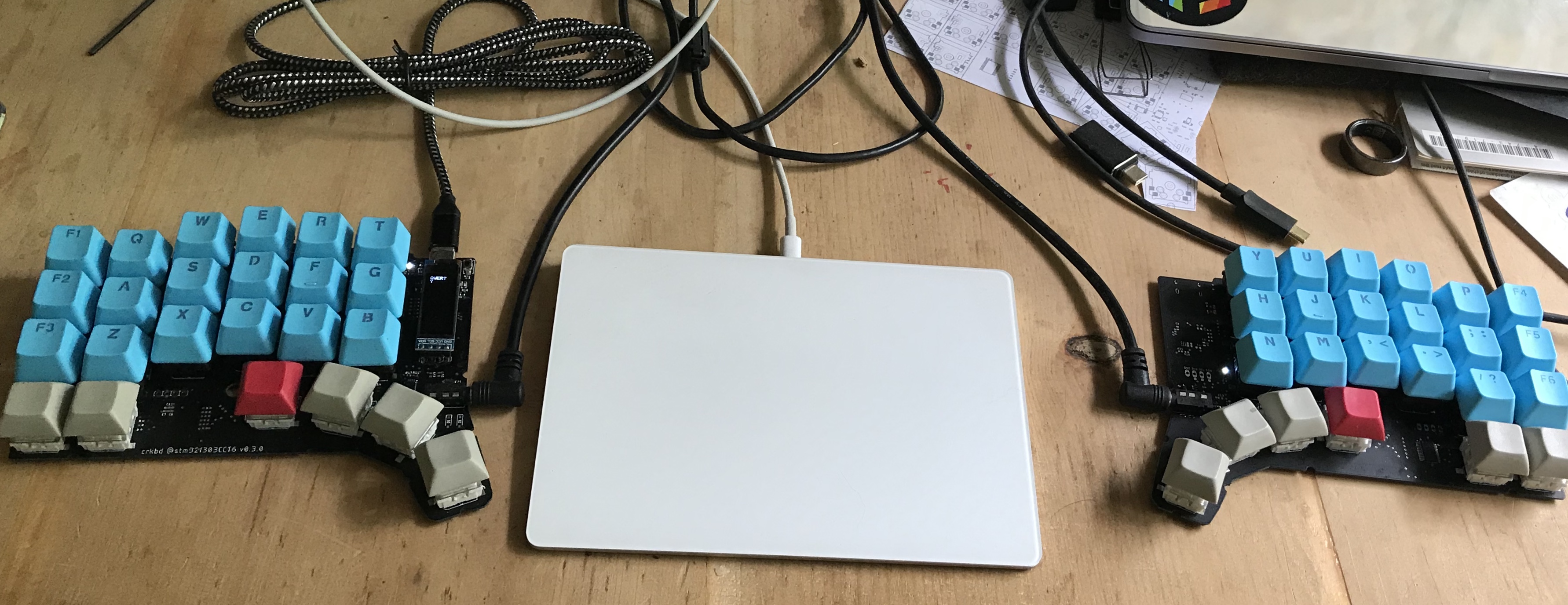
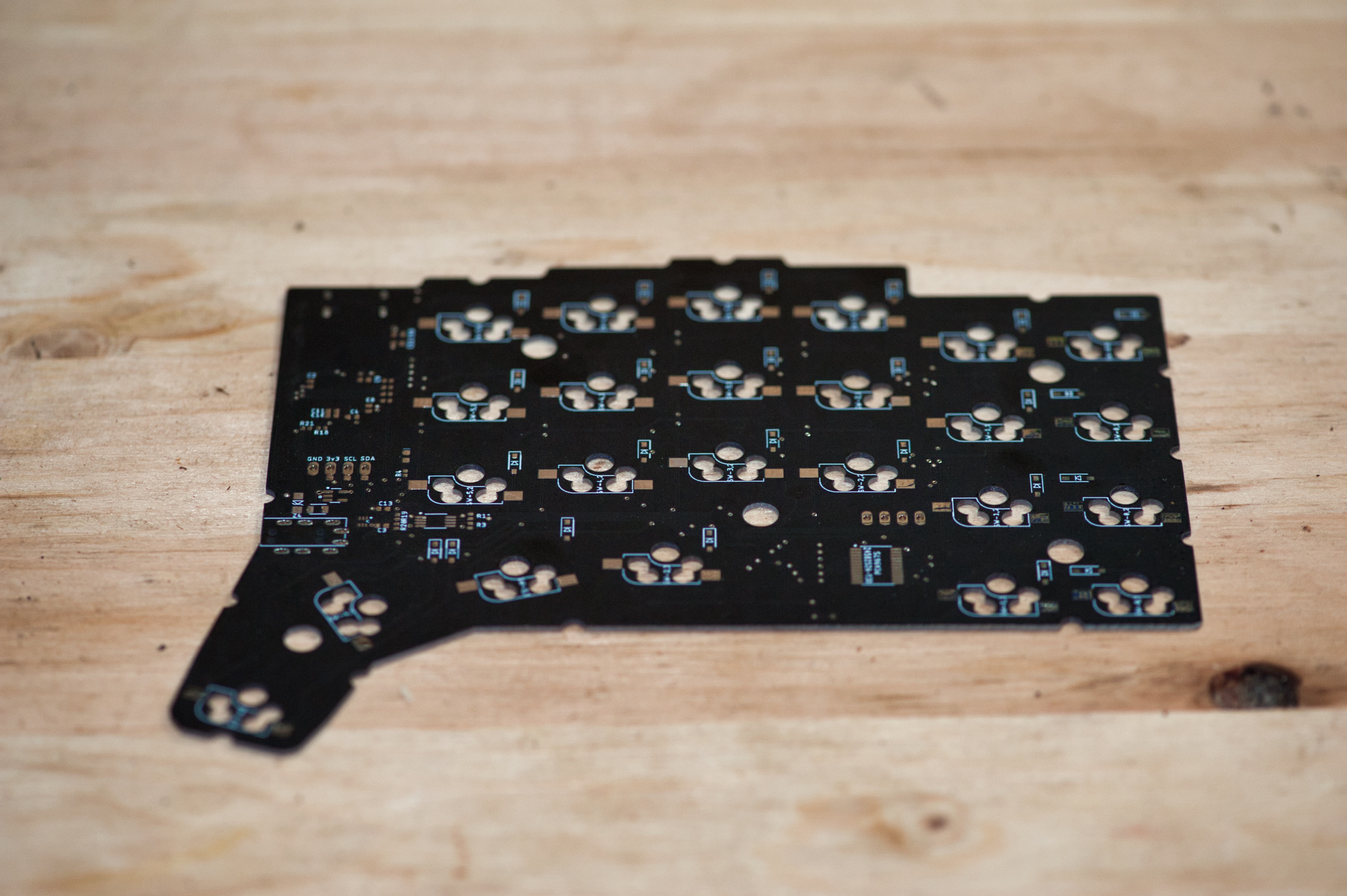
Left Side:
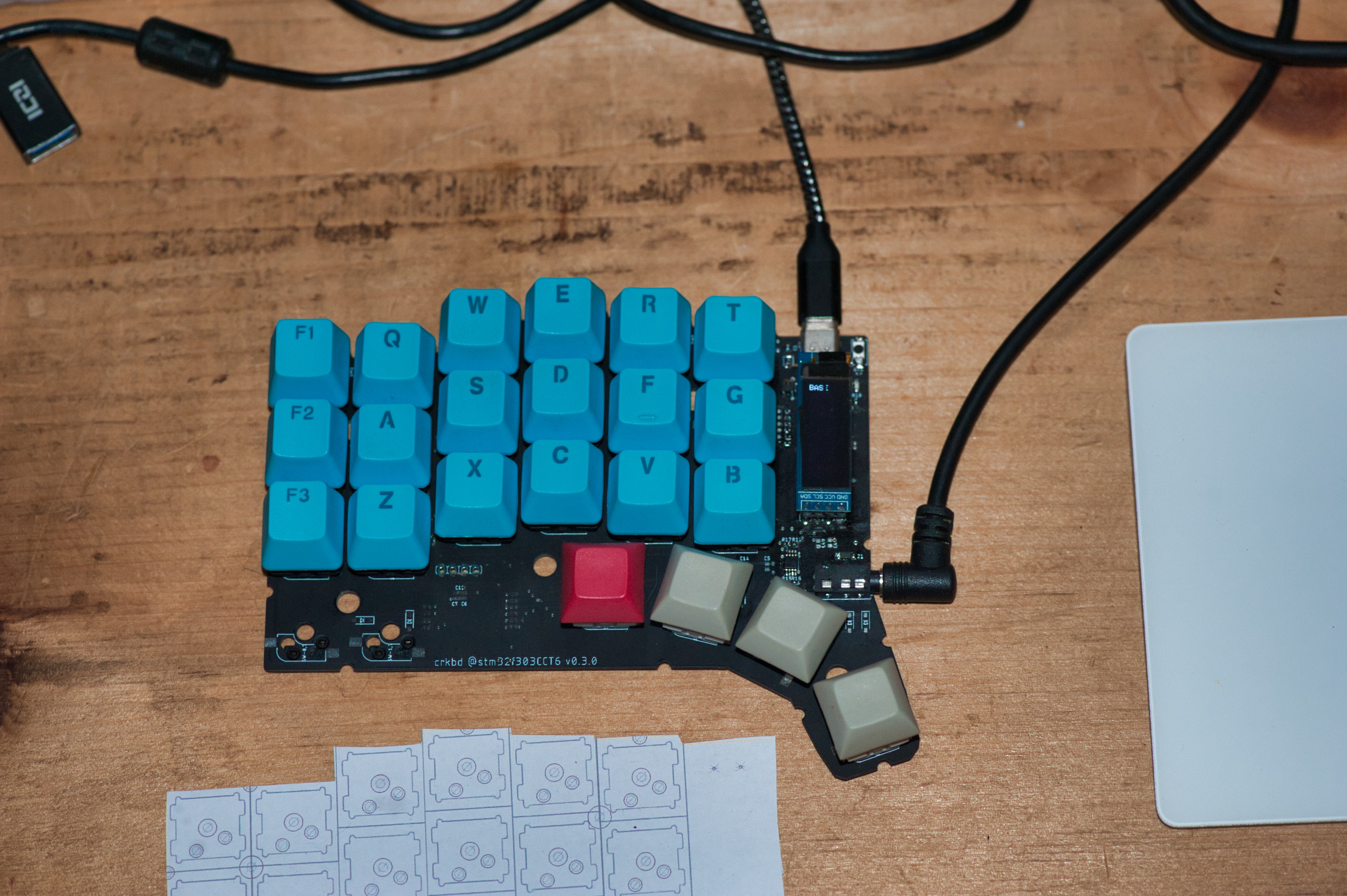
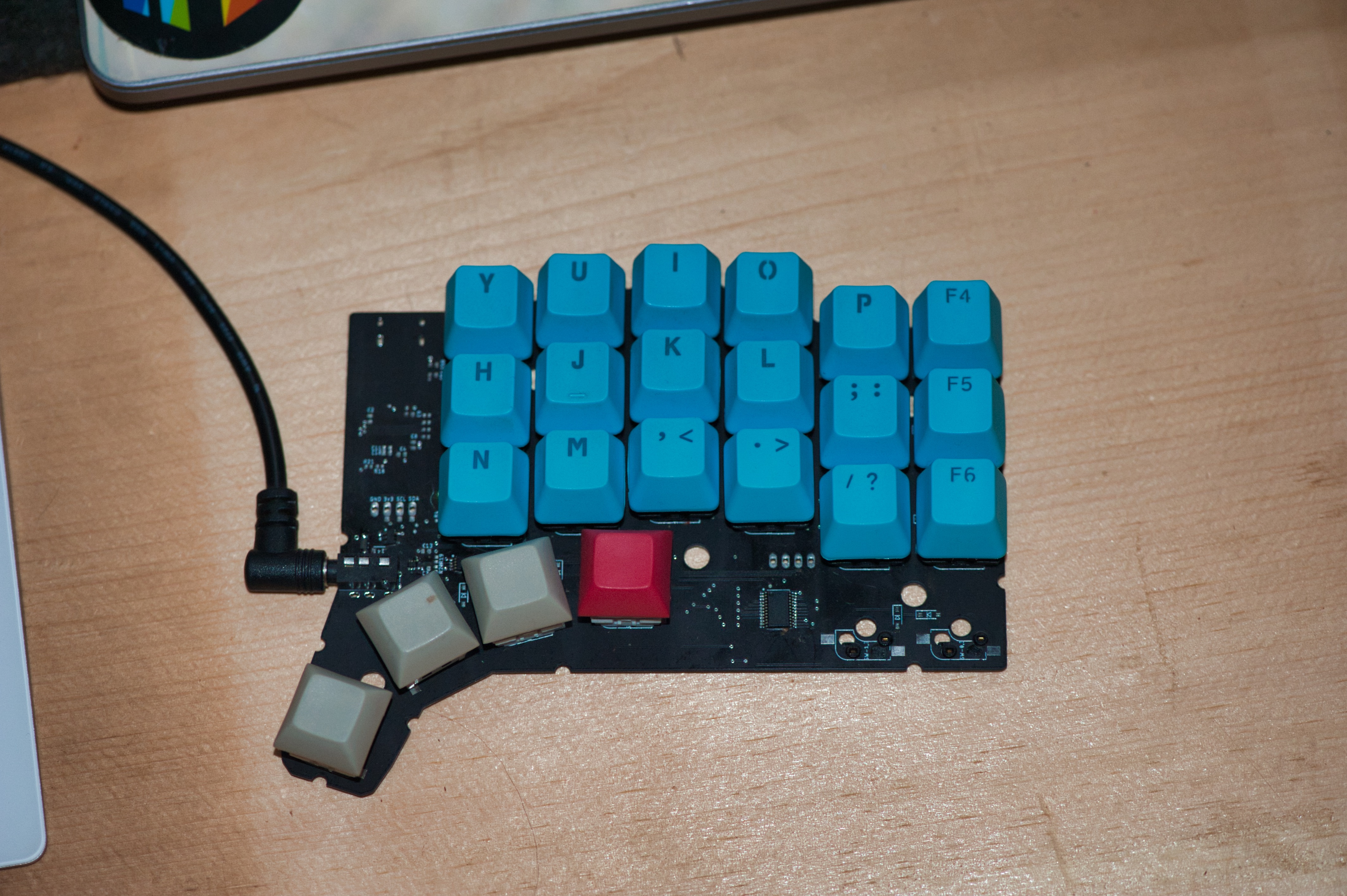
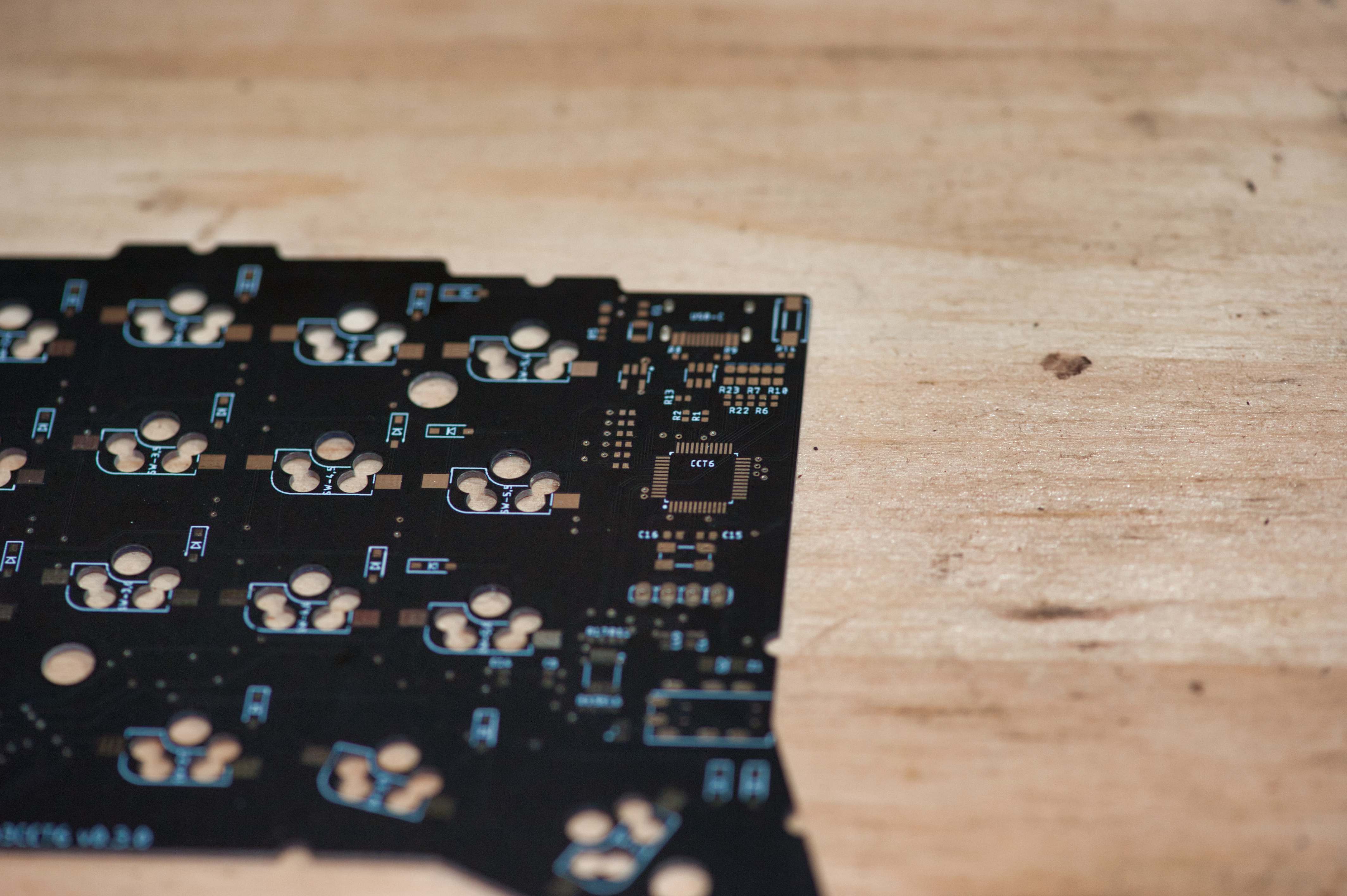
Right Side:
Now, building this took me some time, mostly because it’s been a while since it did any DIY electronics project, and also because I never used an STM MCU before. Here’s the rough history:
A failed approach
I started out with the Ergodox EZ as a reference schematic and copied everything over to Eagle, making component changes as I go; This lead to the first revision, which, as I was certain it would work, directly ordered as a PCB from allpcb.
Unfortunately it had errors in the USB setup and voltage regulator setup. I missed a few components and didn’t read the datasheet for my replacement component close enough. Despite cutting up the PCB and soldering stuff on I was not able to fix it.
While debugging I had a lot of aha-moments, mostly around my own assumptions; I wanted to tread the 3v3 Stm much the same as any 5v Atmel MCU. This doesn’t work as many components want 5v, making working with the Stm chip more involved.
After spending about a month debugging this revision I dropped it and moved on;
Another failed approach
With the learnings from the first revision I updated the schematic; corrected the USB-C setup, dropped the components I didn’t know how to support for now (split RGB using SK6812). Checked all the datasheets, twice;
The 2nd revision was ordered, shipped, assembled. Turned out I missed the USB-C orientation resistors, but that was easy enough to correct. This revision detected the STM32F303 just fine; but something was wrong with the I2C buffers (P82B715 at the time).
I debugged just the right side (MCP23018 at the time) using a raspberry pi. The MCP23018 was working fine. Again time passed, I tried all kinds of things debugging the issue with the broken communication between each side. Again I dropped it.
This was a super useful experience as I learned a lot about the QMK debugging features - though I’d rather have spared me the trouble.
I wish I had had a oscilloscope to look at the I2C lines; not going to spent that money on a hobby though.
A local makerspace is probably your best choice for this. I went another route though.
Switching things up
Apparently it’s very easy to have small errors creep in. So instead of ordering another round of biggish keyboard PCBs I designed a small number of breakout boards, each purpose build per the respective datasheet; I also expanded the ICs I considered a lot, both for I2C buffers and I/O expanders.
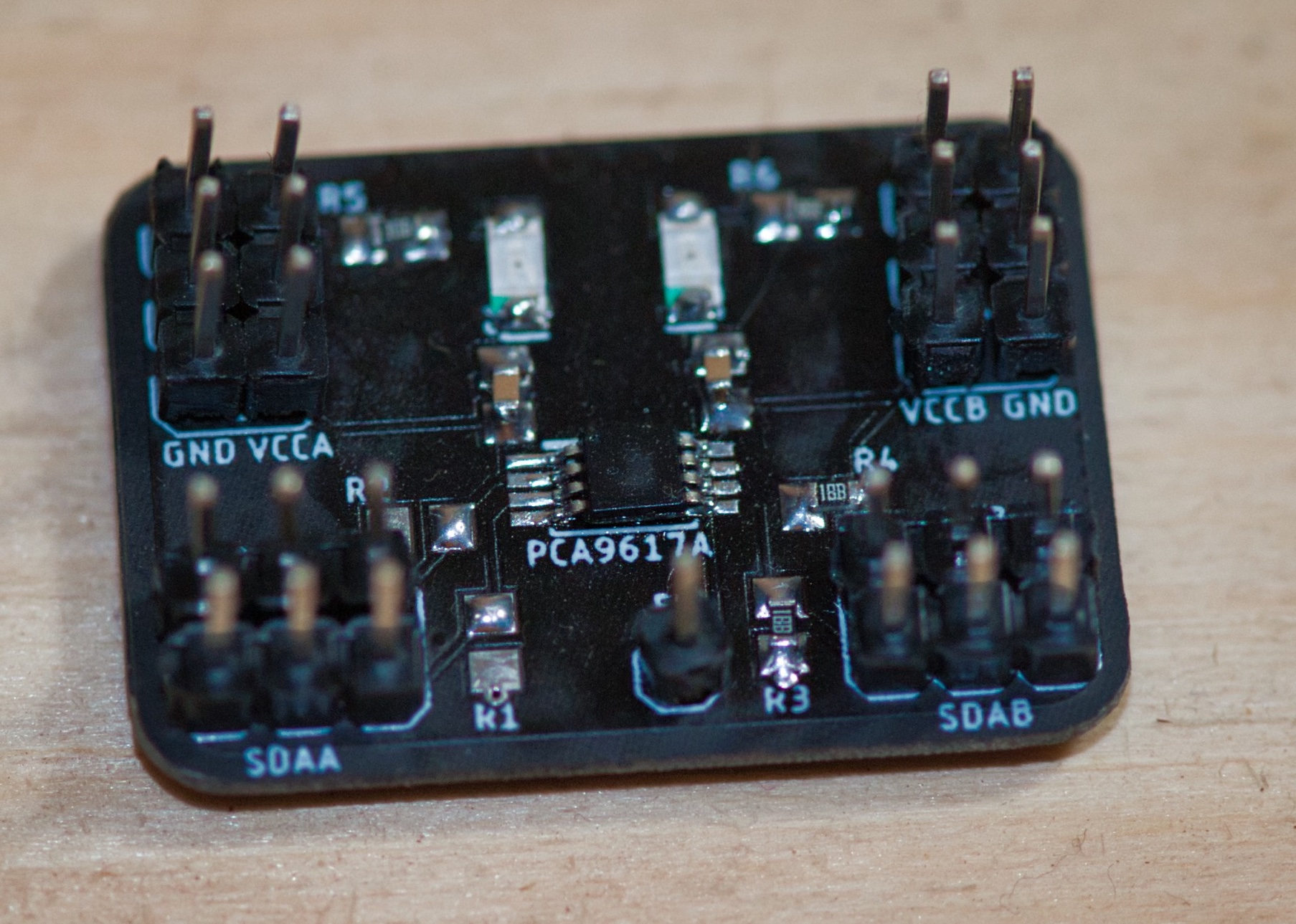
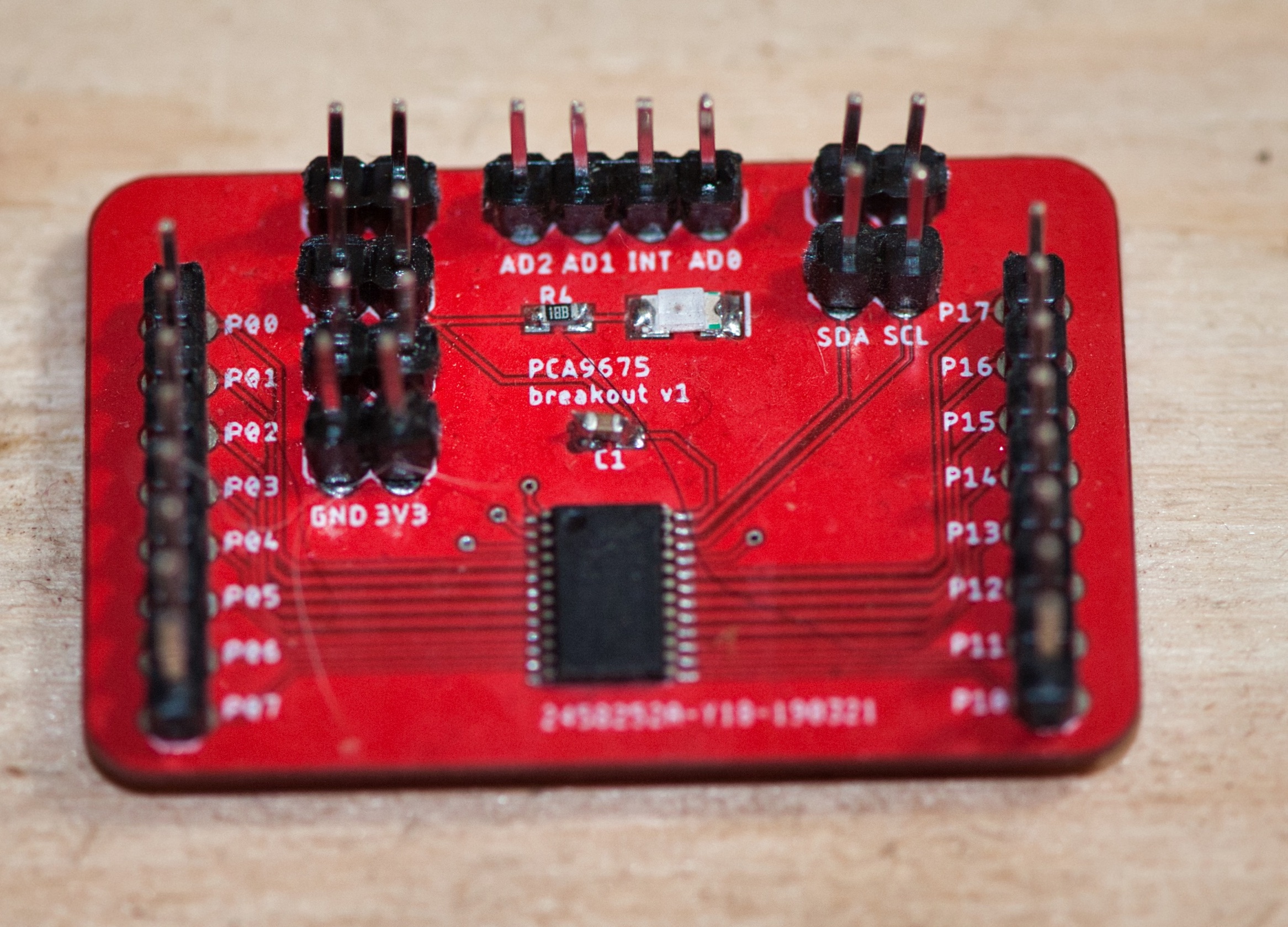
I double, triple checked all datasheets. The first revision of each breakout board instantly worked. Having all these breakout boards for the SMD components allowed me to quickly assemble a completely working split keyboard using QMK. I swapped out the i/o expander for PCA9675, which is much easier to integrate than the MCP23018, and replaced the I2C buffer with the PCA9617A, as it supports higher I2C speeds per the spec
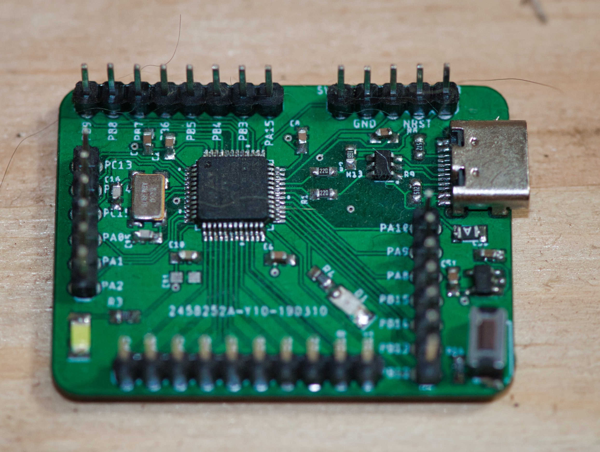
STM32F303CCT6 breakout board
PCA9617A breakout board
PCA9675 breakout board
Now building the breakout boards helped me both improve my component placement and manual routing skills, besides ending up with an ugly but working hand wired prototype.
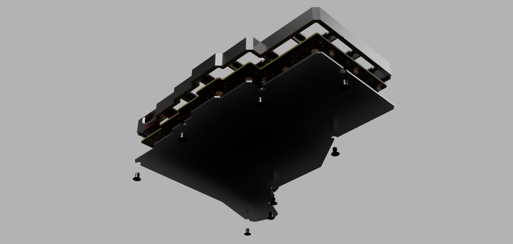
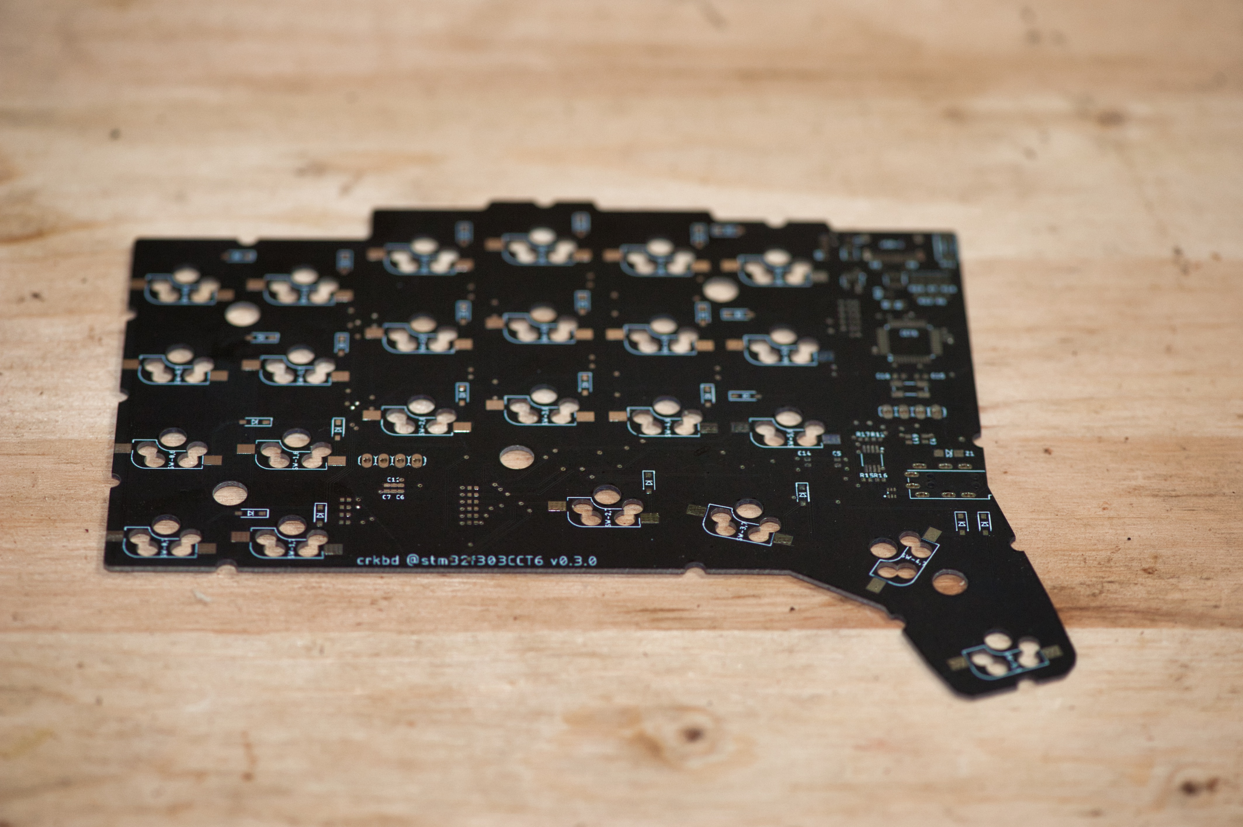
I merged everything back into a single PCB, and finally:
success
Ganymede rev 0.3 in all it’s glory
left side:
flipped, right side:
close up
because I knew what to look out for in the component placements after working on the breakout boards I was confident enough to reduce the size of most components for this revision down to 0402s. All breakout boards used 0805s or 0603s; however, space is a rare resource when you want to have your PCB flippable, so reducing the component size allowed me to make it easier to solder as you can increase the distance to the next nearest component a little.
Still, 0402s are tricky to place and solder.
A nice thing about the flippable PCB is that I get 5 pieces at MOQ, which allows me to solder 2 working keyboards per revision, with one spare PCB for test soldering - in case I mess up.
next steps
I’m currently working on revision 0.4 which will incorporate IS31FL3733 based RGB lights, and I’m following the same approach: first, getting a working breakout board, then, integrating it into the design.
I think this is a solid approach, which reduces the chance of wrong schematics to just the component I am looking at integrating, not the entire thing:
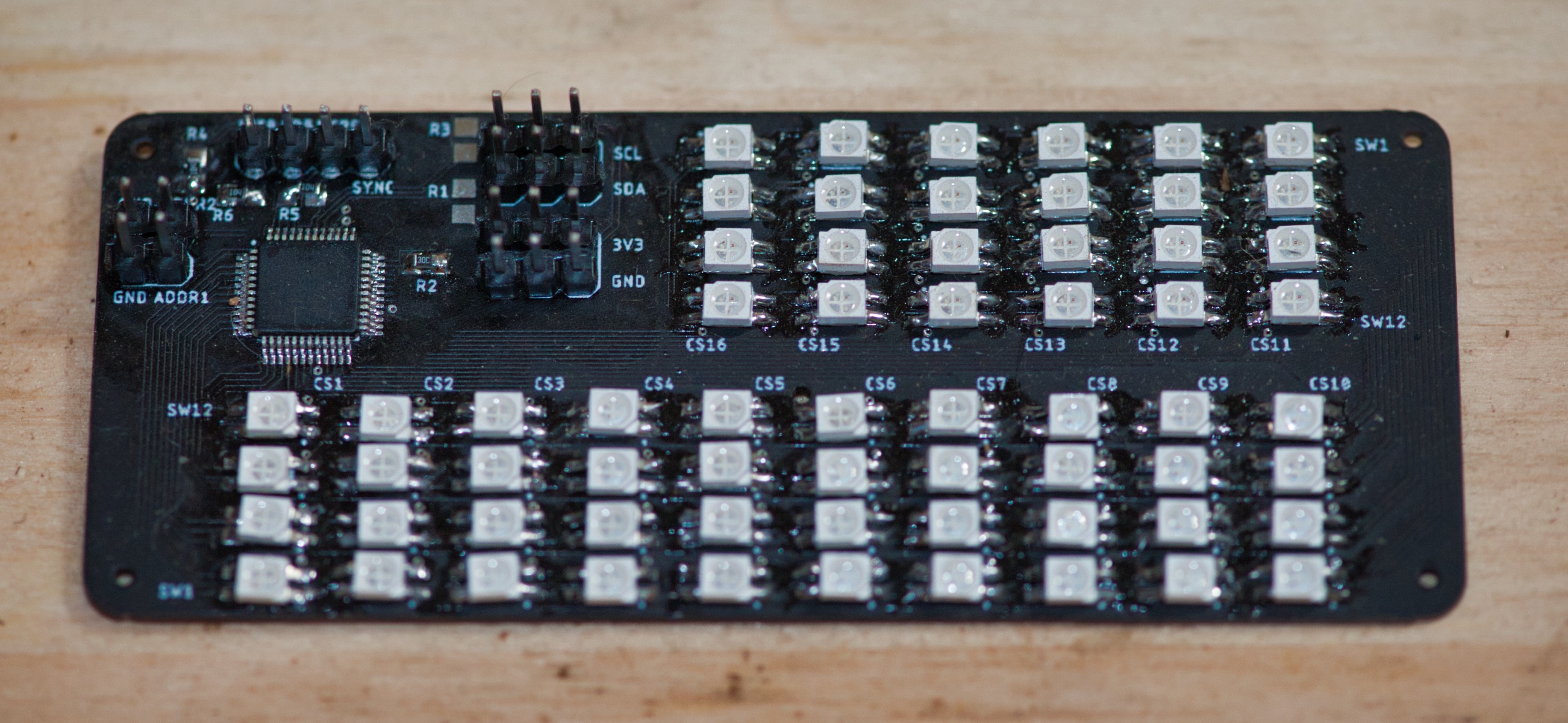
IS31FL3733 breakout board
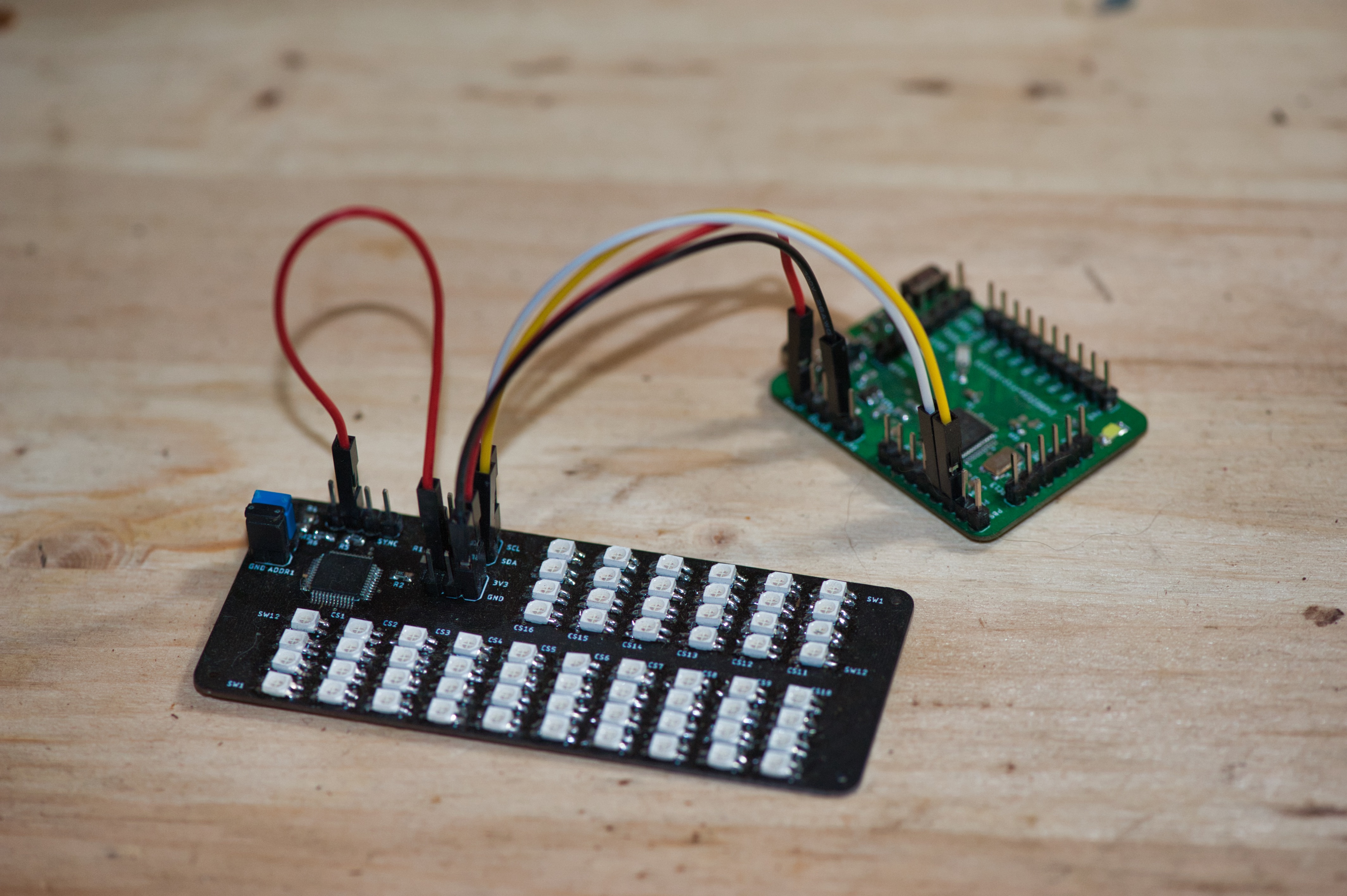
hooked up to my STM32F303 breakout board
Besides the incremental approach to component integration I also started prototyping keyboard layouts using my good old paper printer:
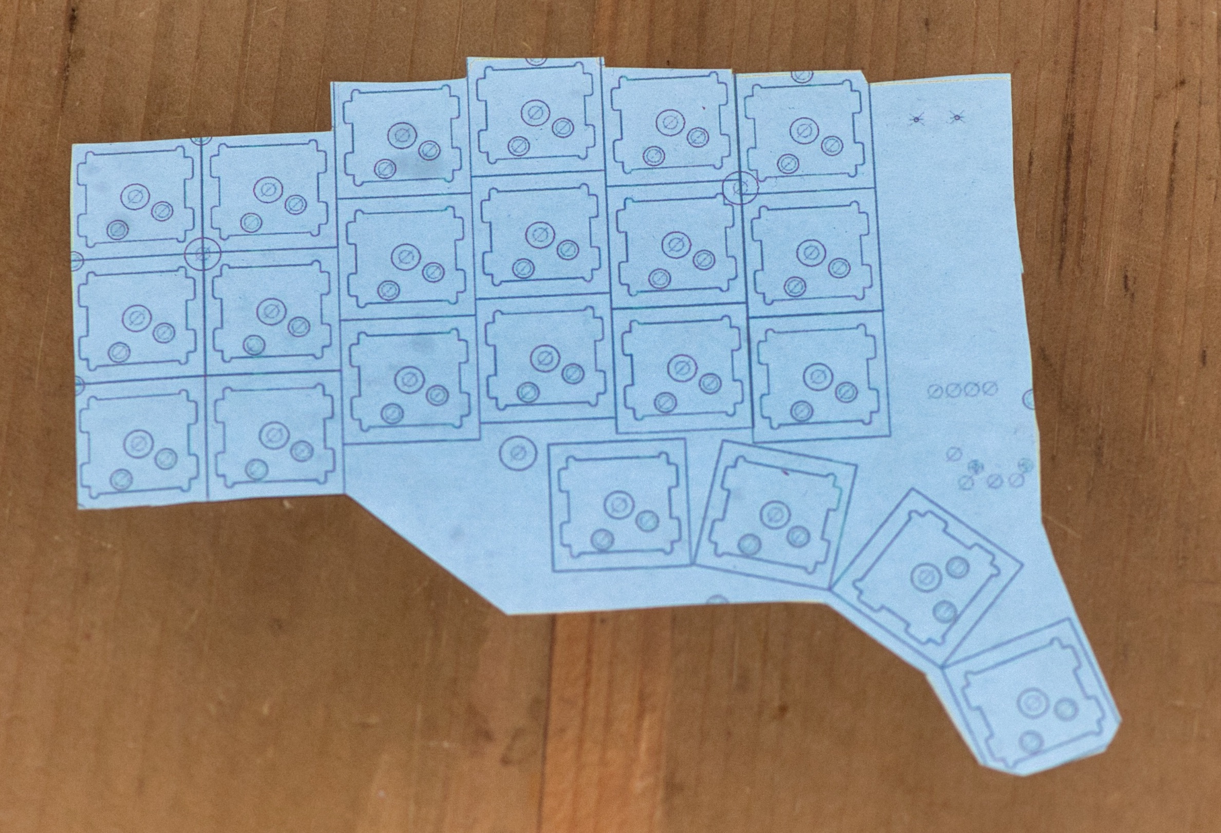
It’s a useful idea to cheaply play around with layout options; This is how I’m going to change switch placement in revision 0.4, as I can’t reach the lower two switches with my pinkies easily.
Summary
- always check your datasheets. not once, twice, but three times. then take a good night of sleep, and take another look at your schematic; also, prefer official product datasheets over any guides you find on the internet. there are just to many wrong “guides” out there.
- paper prototyping for rough keyboard layout is great. It won’t work to give you the feeling for individual key placement, but it’s close enough
- prototyping SMD components via home grown breakout boards is super useful. Especially since you can place detailed silk screen names, and leave enough room for debugging pins etc.
- flippable PCBs are awesome, but tricky to layout. On the plus side, you don’t need to keep multiple brd files in sync when you move components around.
However, designing flippable PCBs is more involved. It’s probably a separate topic I can dive into more detail separately.
That’s pretty much it - the kepler keyboard is far from done.
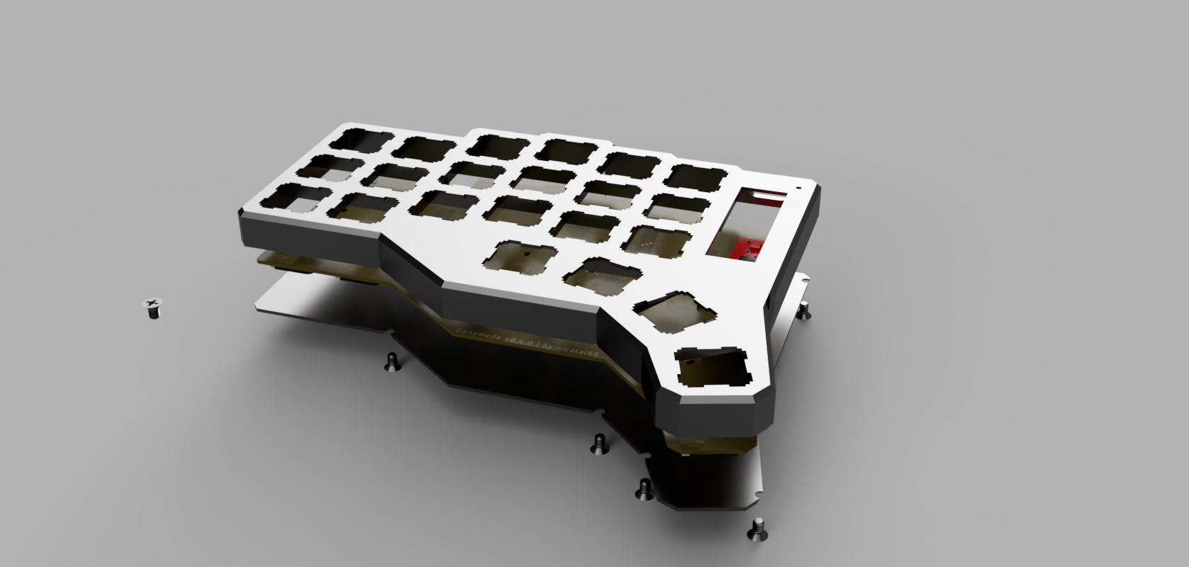
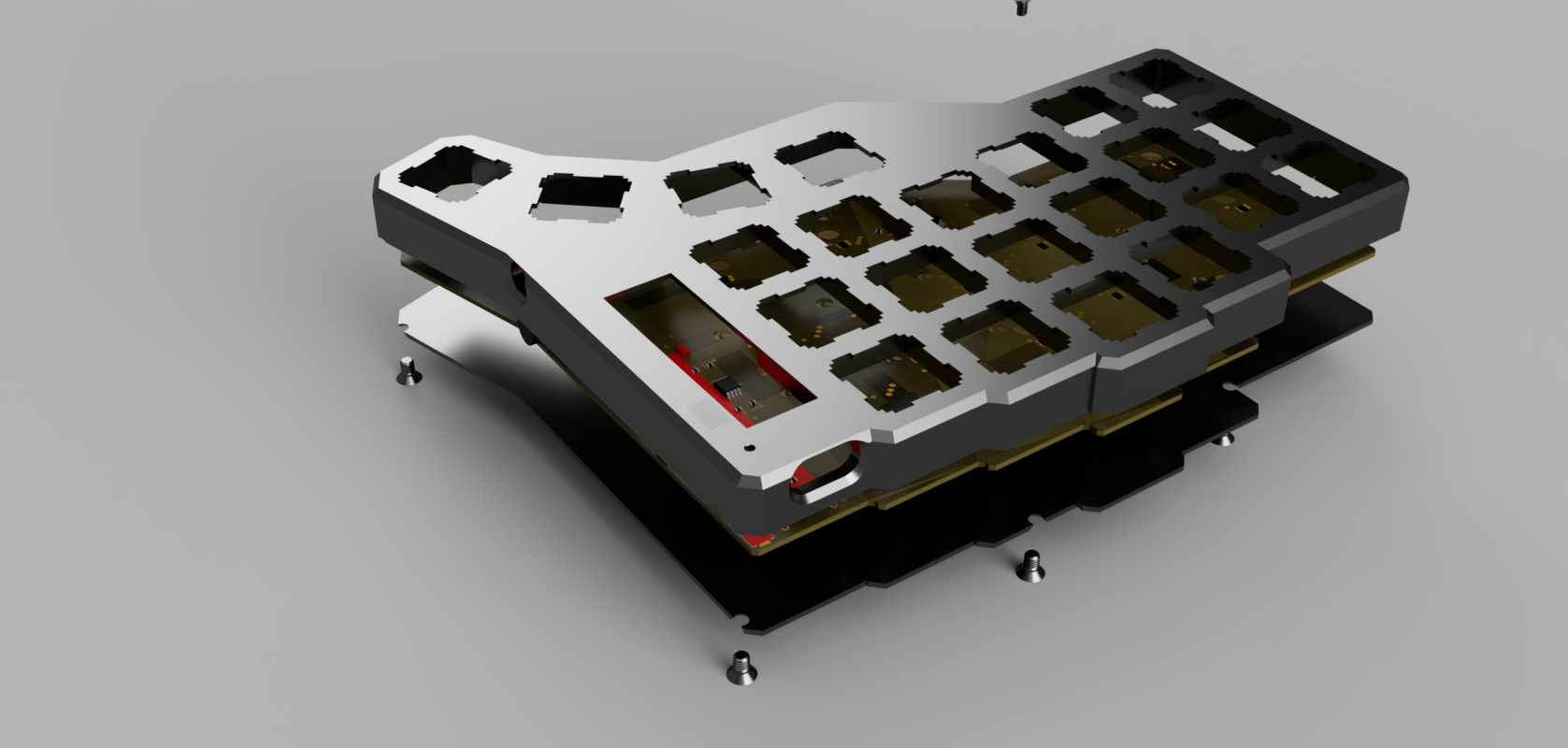
Moving on, I’m working on designing a proper case using Fusion 360, as well as iterating on the design to more closely fit my own hands. If you consider this interesting, take a look at the github repository which contains all QMK code, schematics and gerber files for the current iteration.
I’ll keep this thread updated as I move my way through Fusion360, all the way to a CNC’d case ![]()