The Winghead, a new personal keyboard project

Hello keeb lovers,

As a way to entertain myself and learn new things I started designing and making my own keyboards last year.
It has been a tiring and sometimes frustrating experience but I learned a lot in the process.
I now use my first homemade custom at work for nearly 6 months and I’m still surprised to find it better than my old Filcos and Topre boards.
It is my ‘precious’ :smiley:
If you are curious, the history of the project is on this forum at this link:

I thought that this endeavour would discourage me to go further … just to discover that I was eager to start another design shortly after :slight_smile:
Plus I jumped into the buying spree syndrom that most of you know, and ordered several keycap sets made by famous designers out there :smiley:
I need to have a case prepared for these when they will arrive.

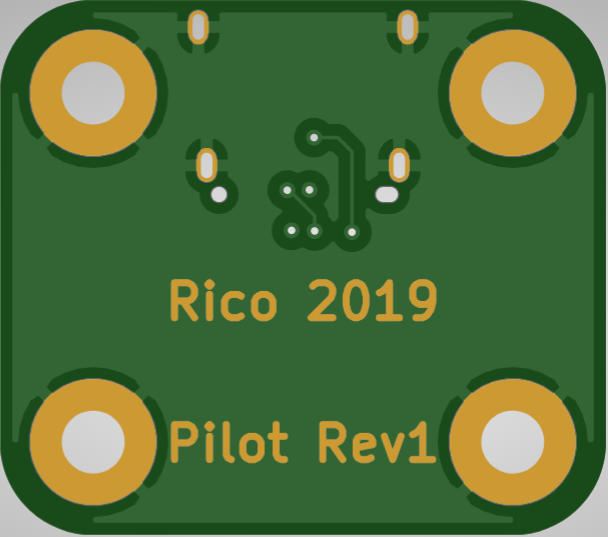
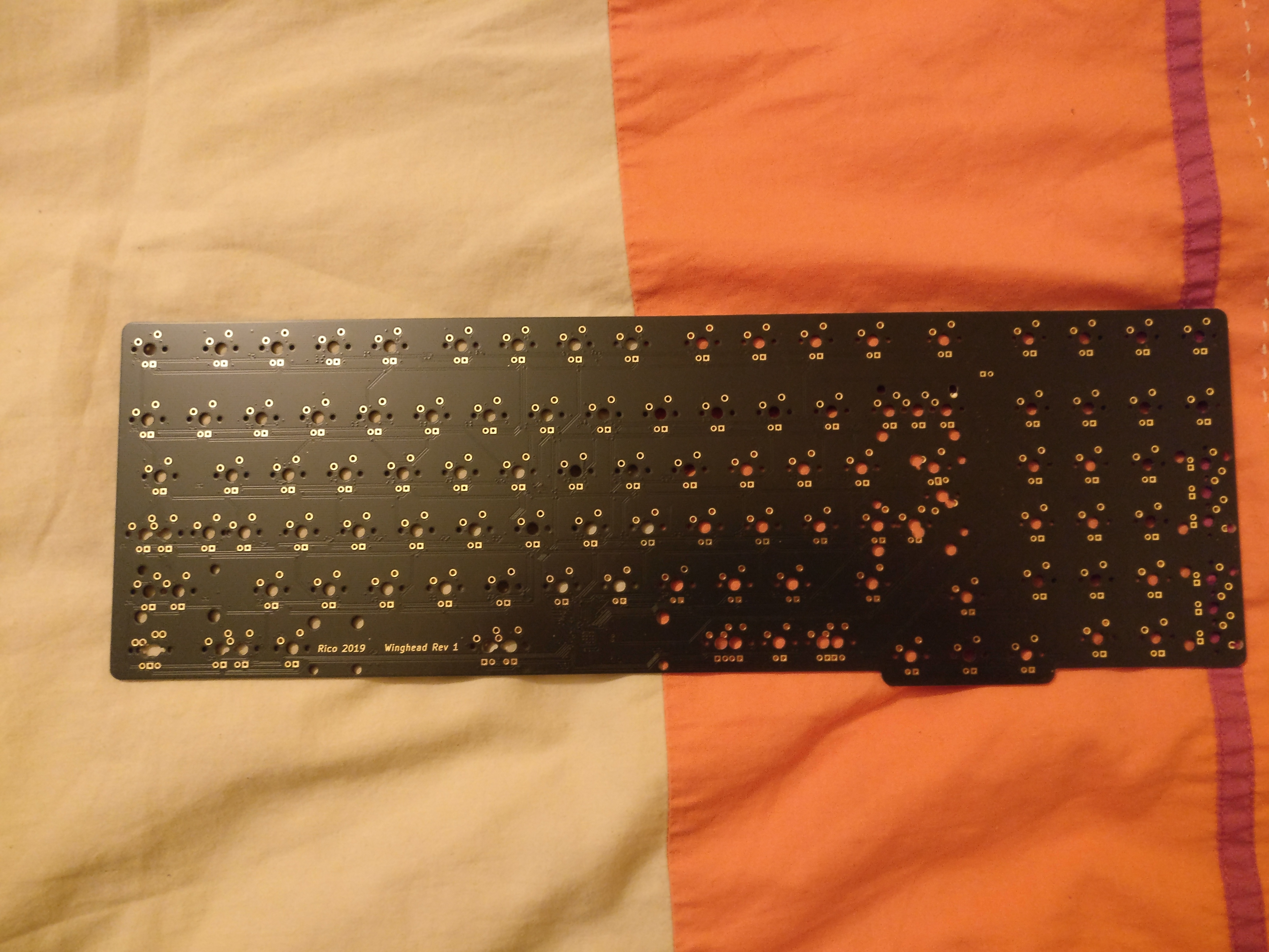
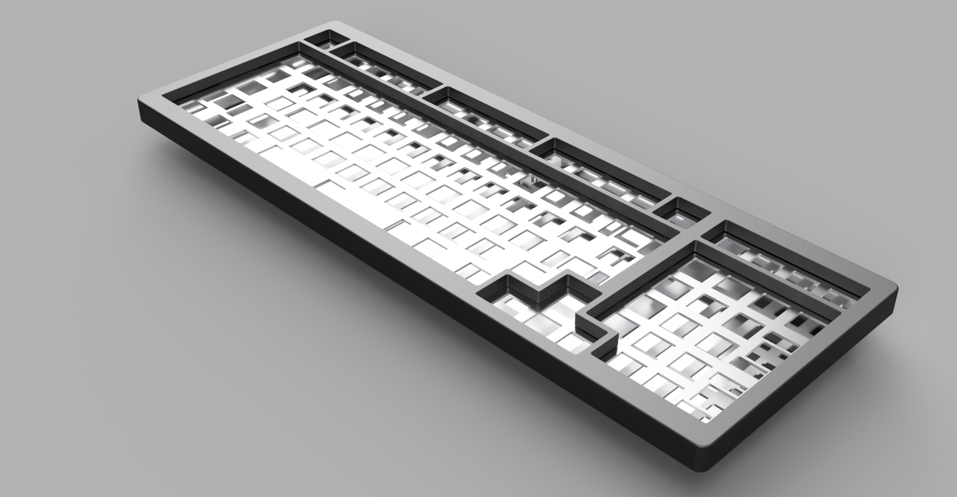
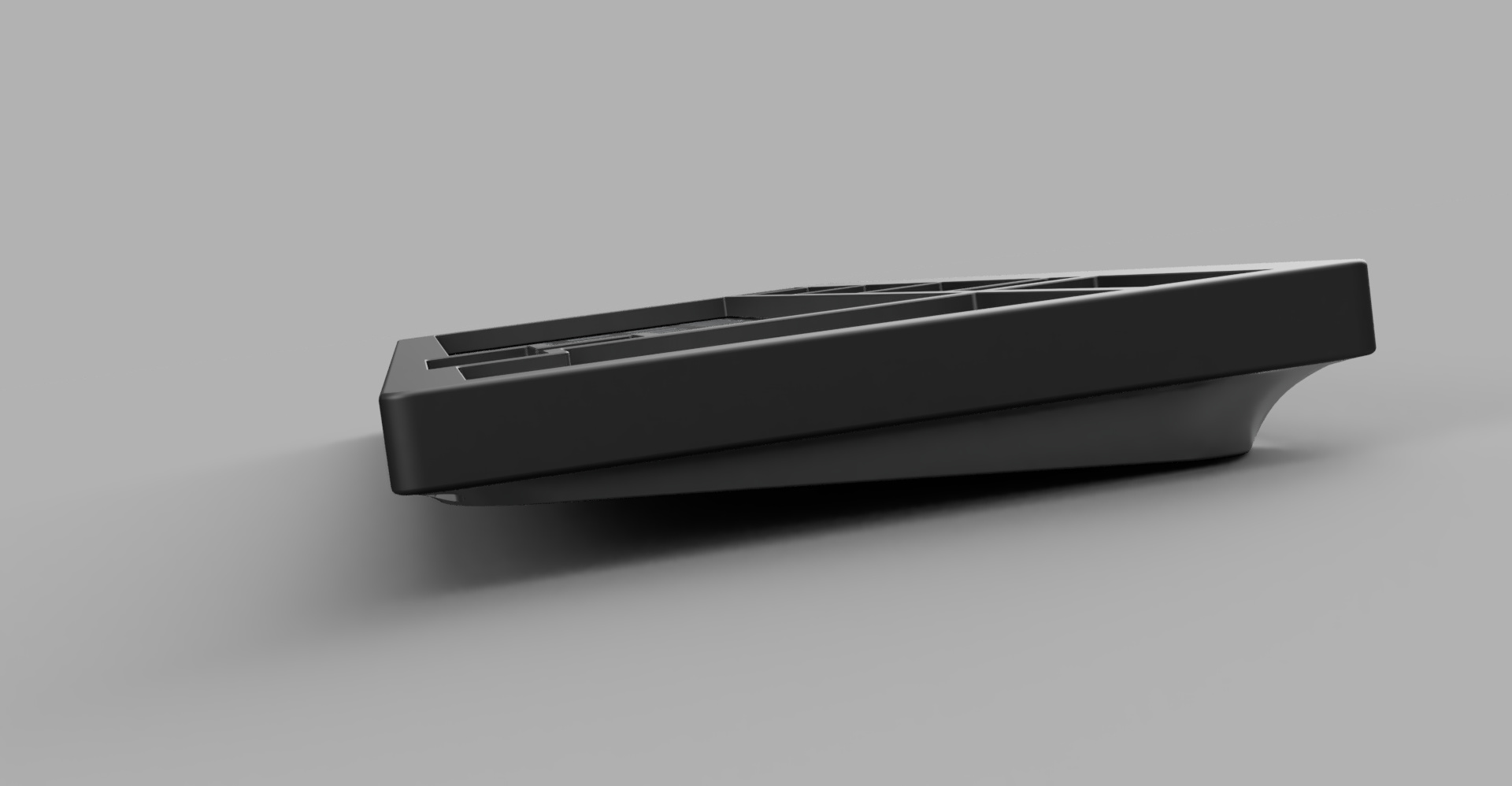
So here is my new project, the Winghead (a special species of hammerhead shark).
It is very new(no more than 2 months) and will take a long time for completion: it took me around 8 months for the previous project to be finished.

What I had in mind for this project:

  • Try a different layout, but not too small either.
  • Increase PCB functionality and complexity a bit to have new challenges.
  • New case design of course.
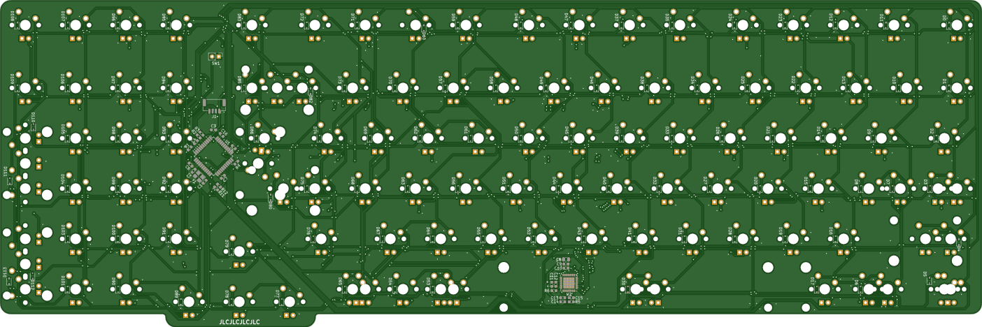
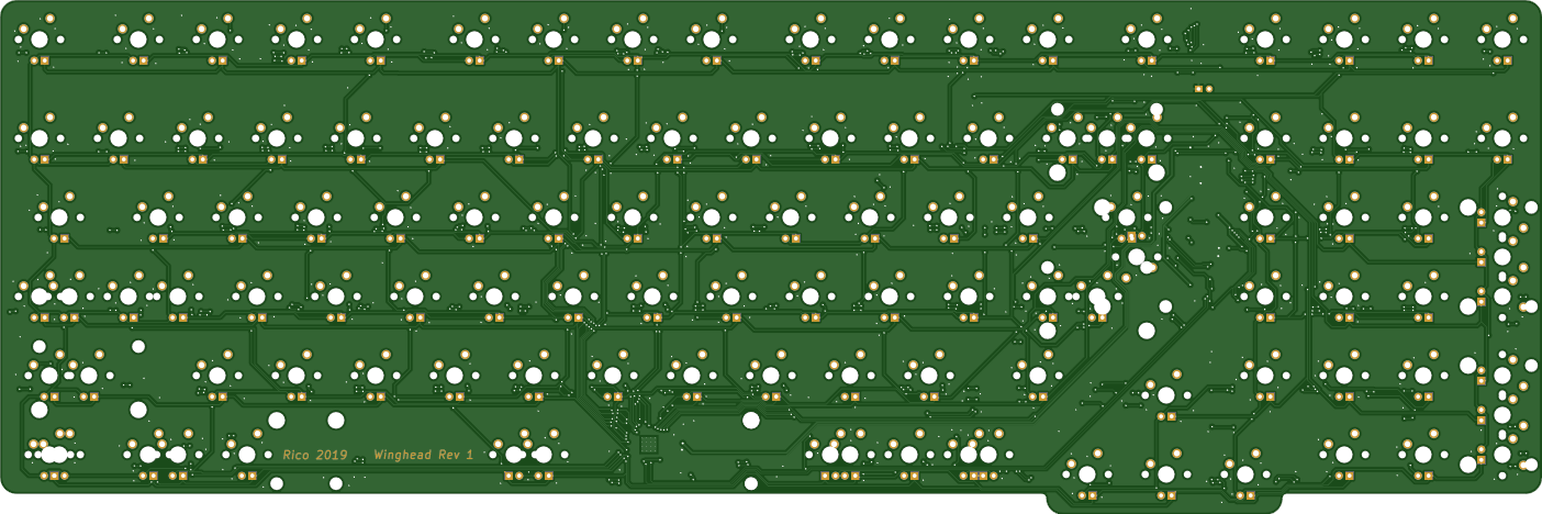
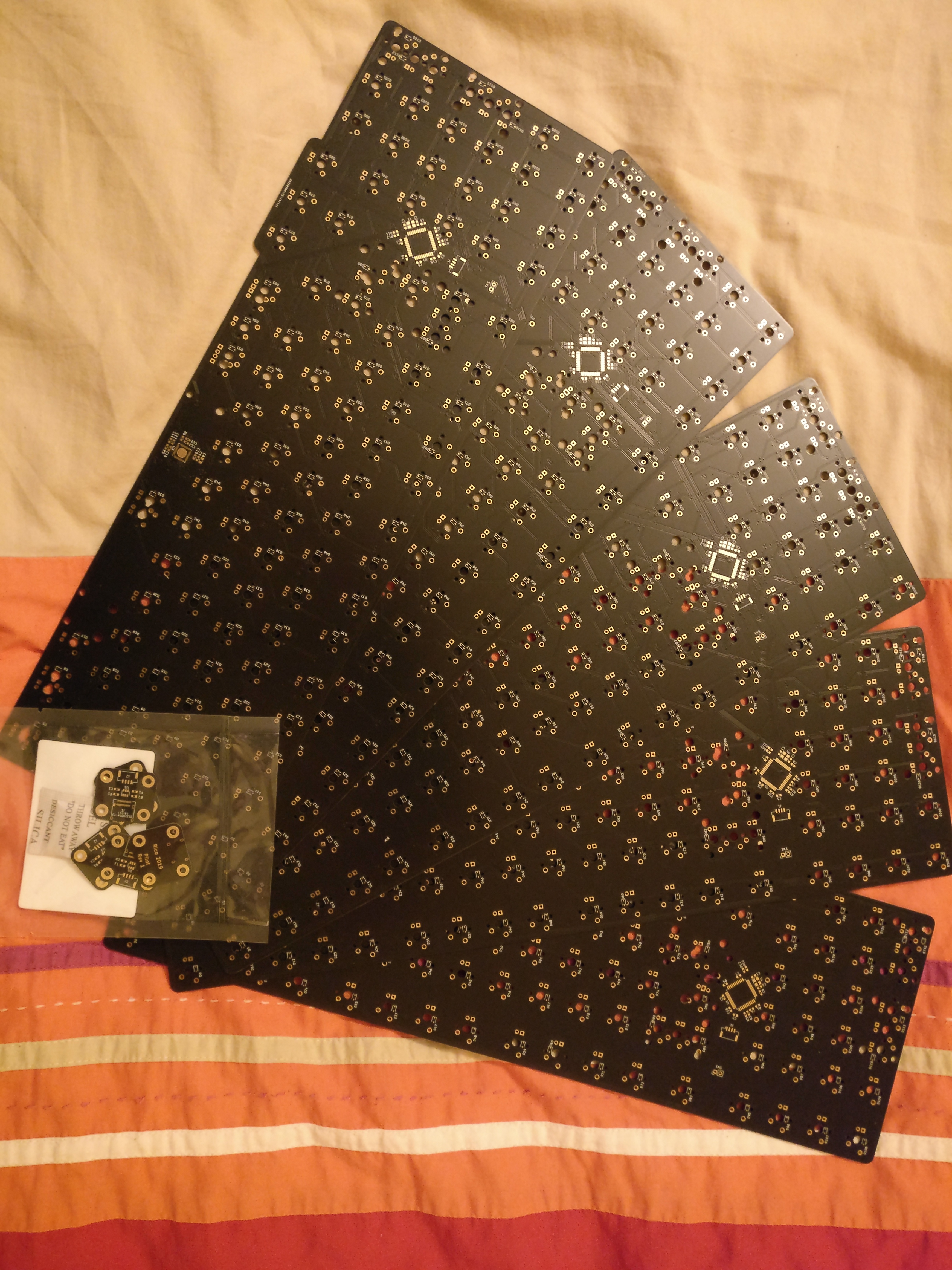
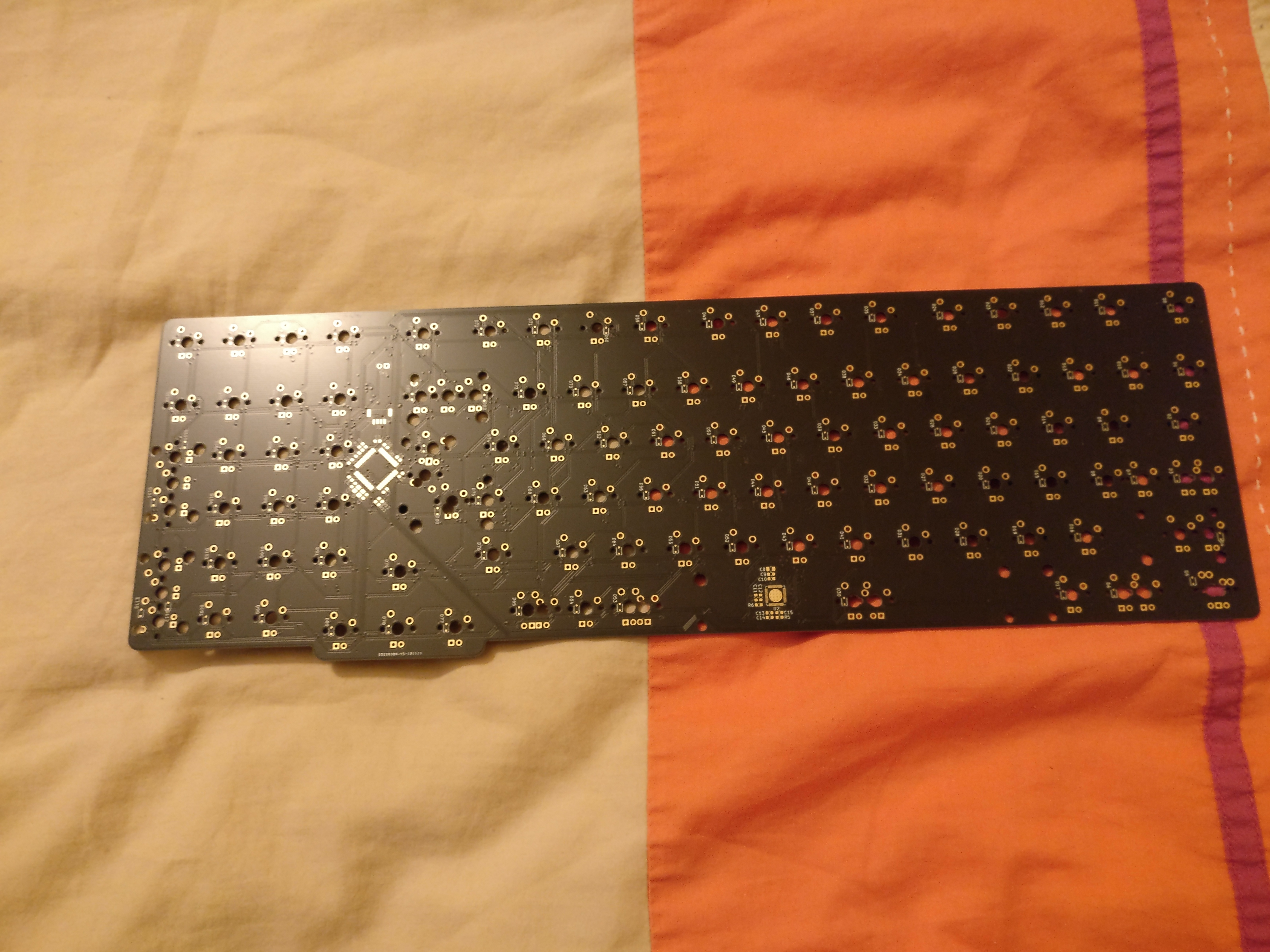
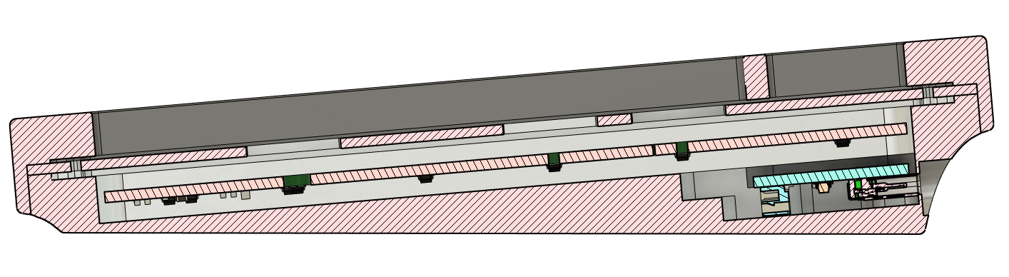
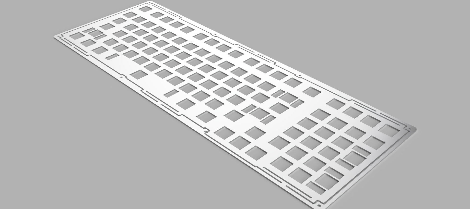
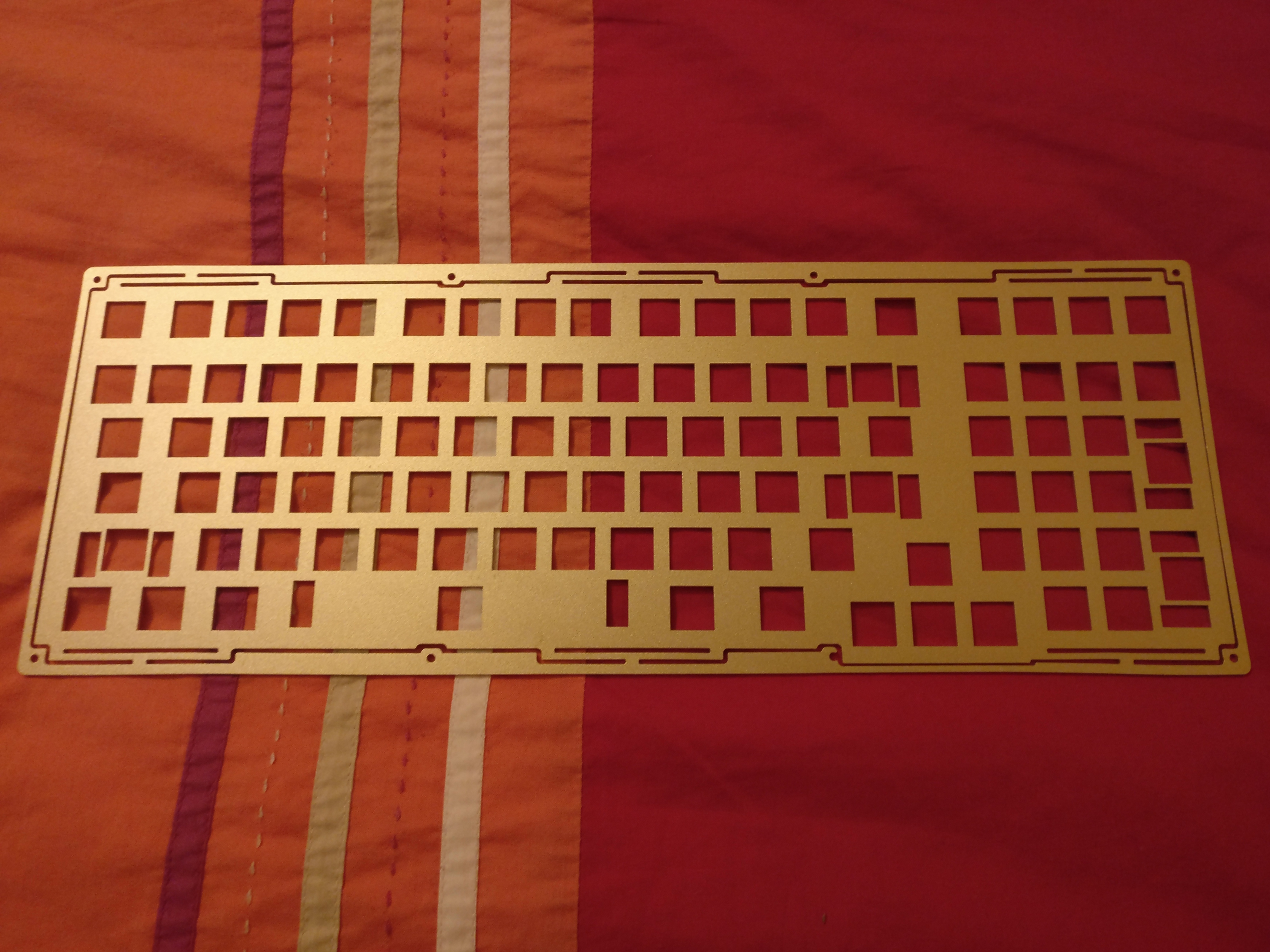
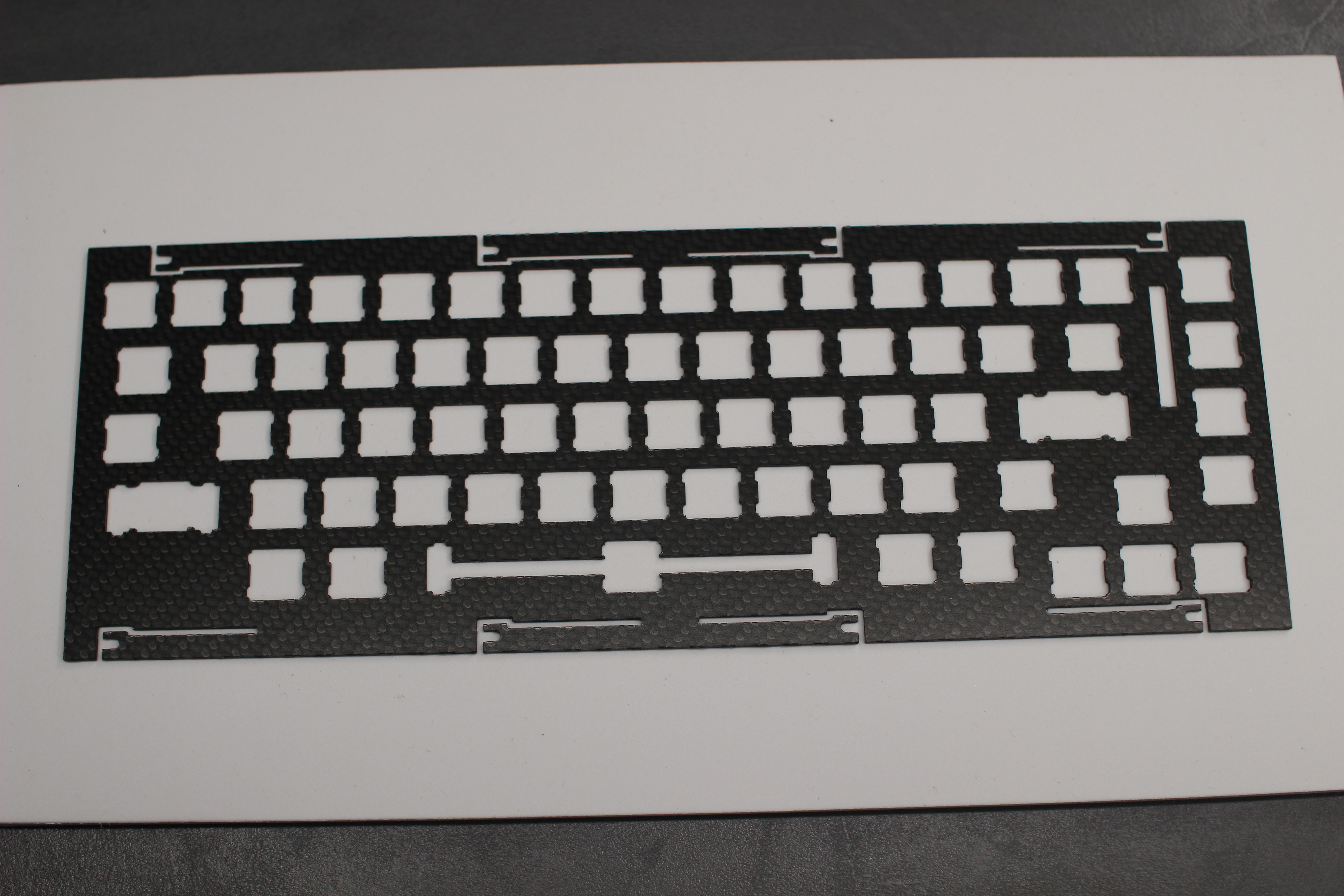
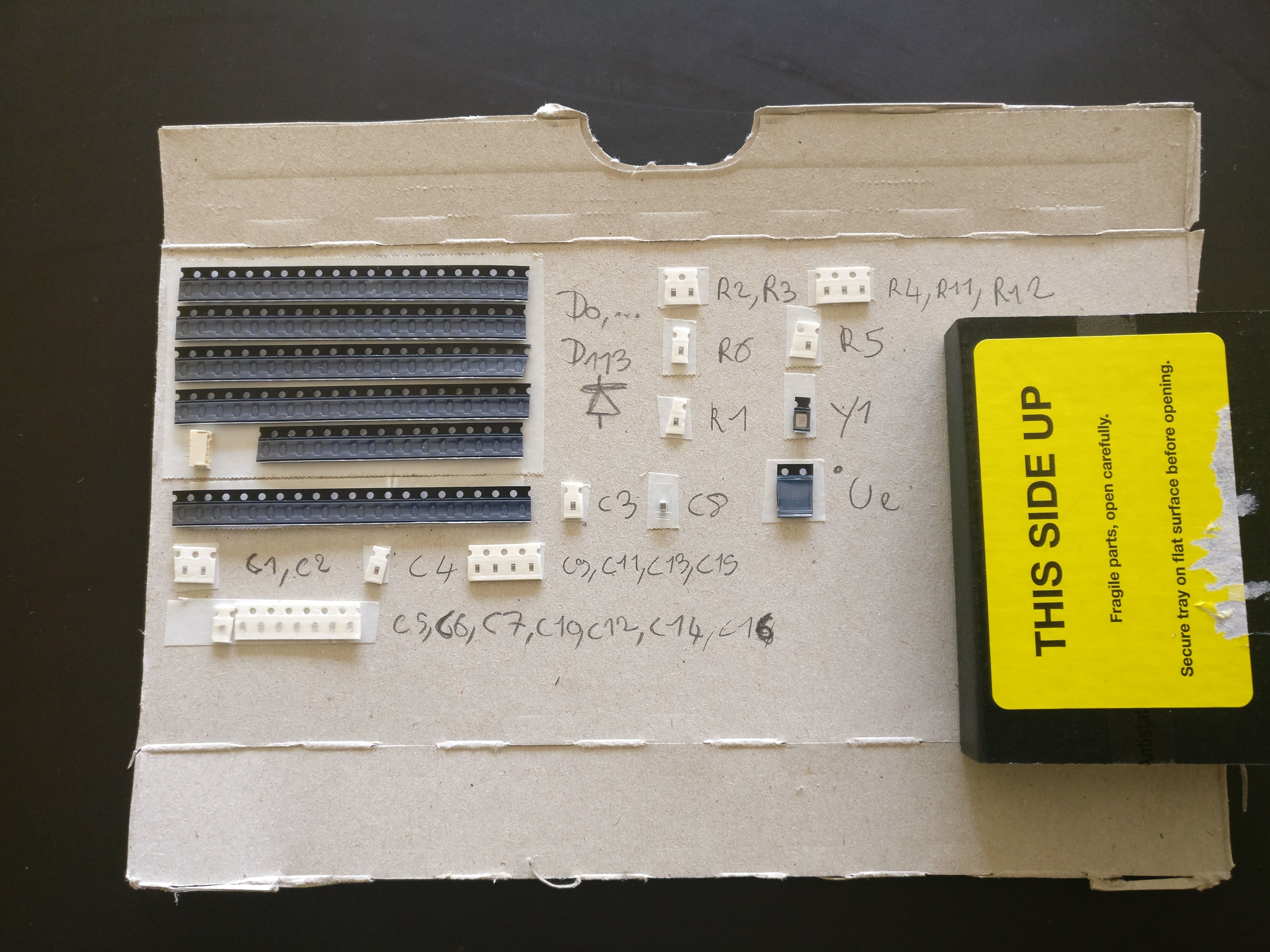
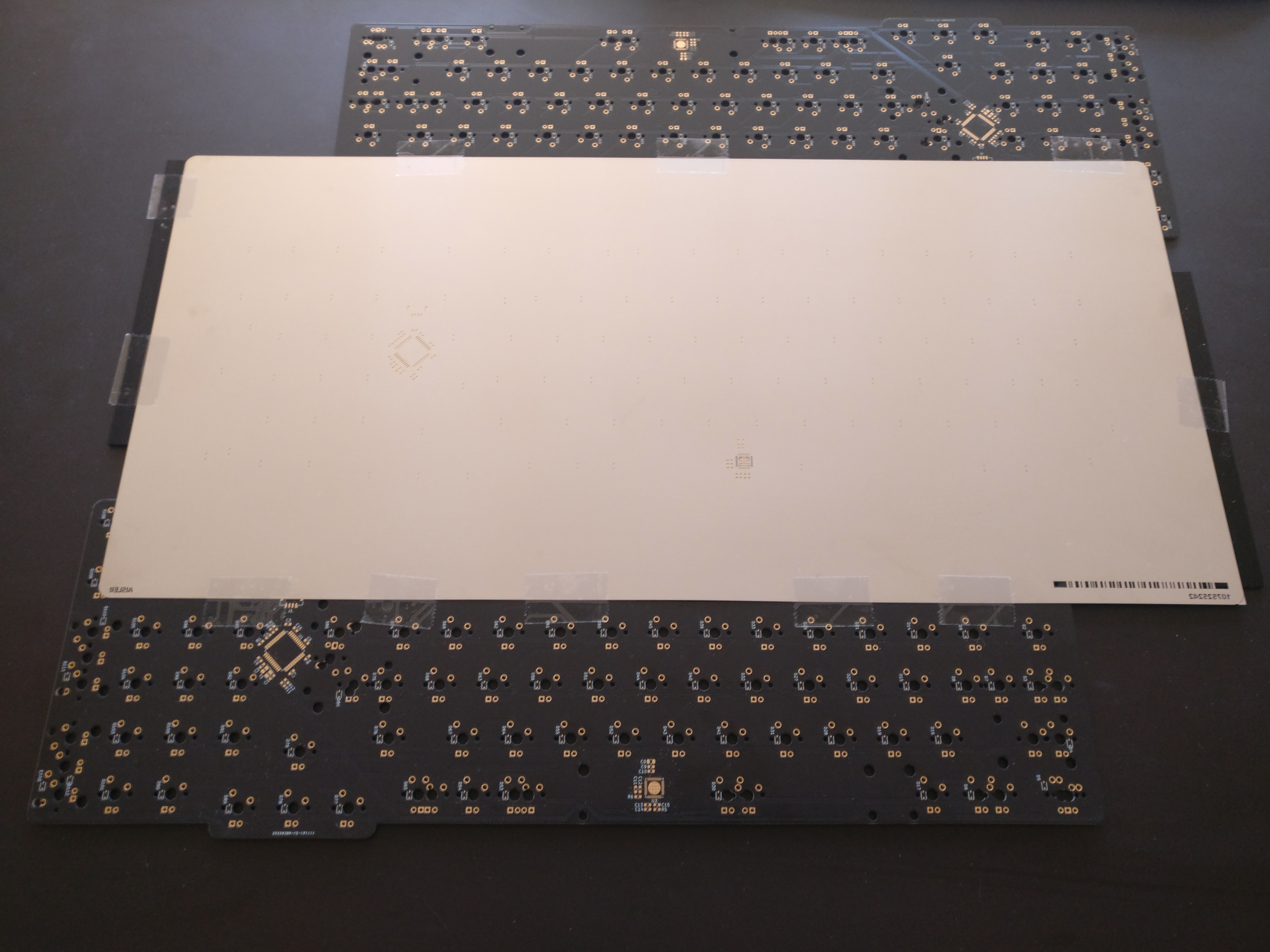
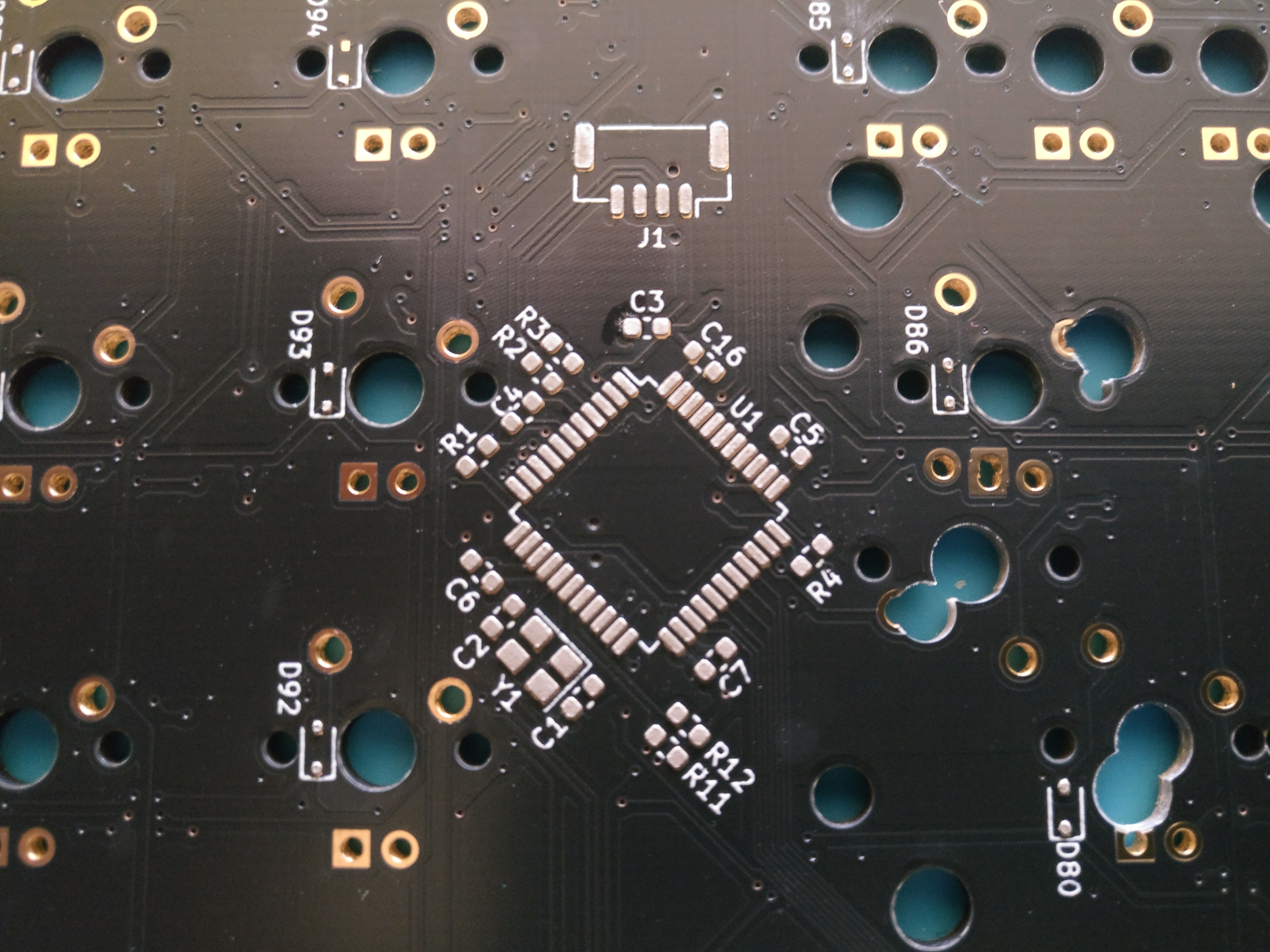
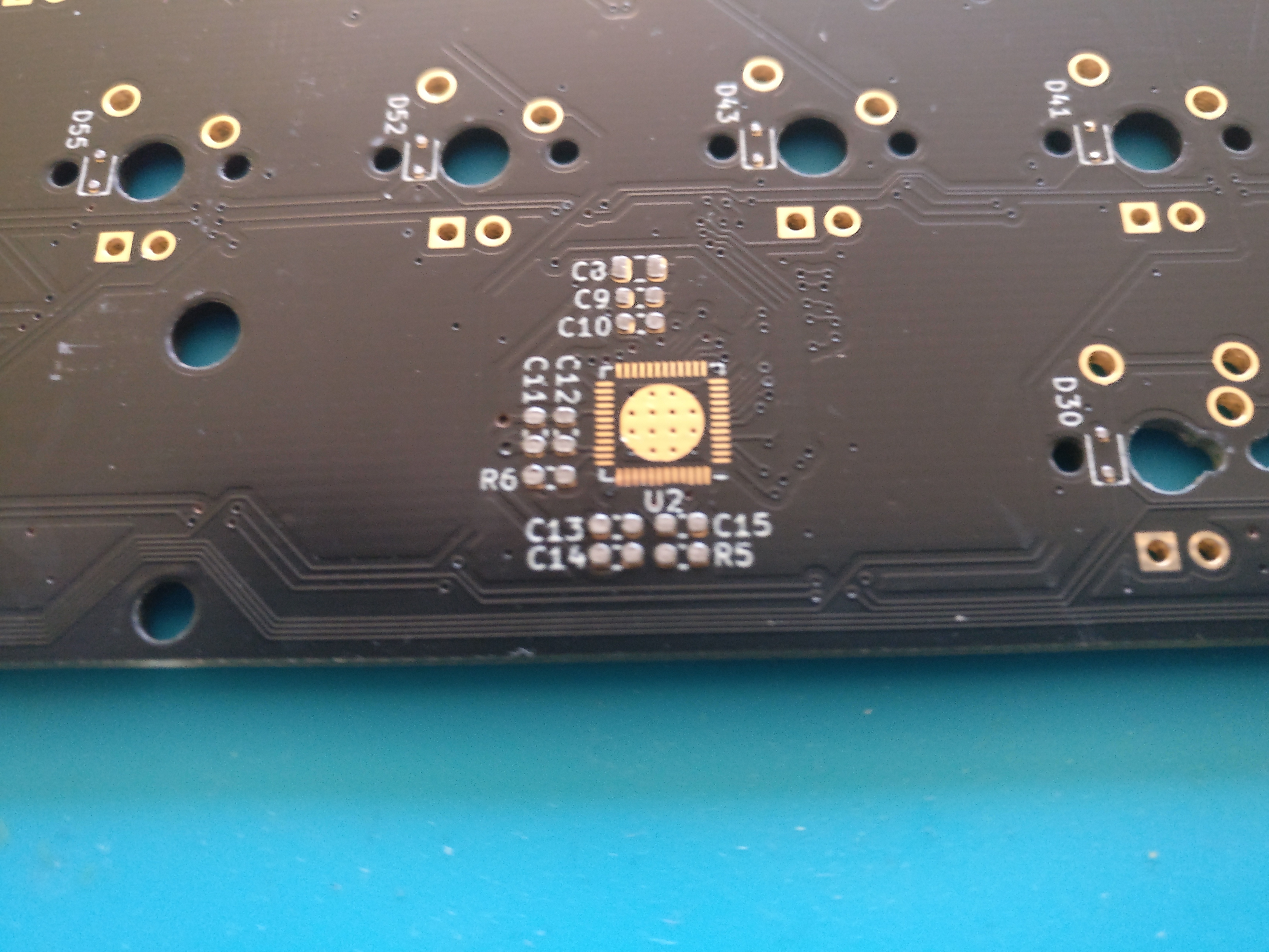
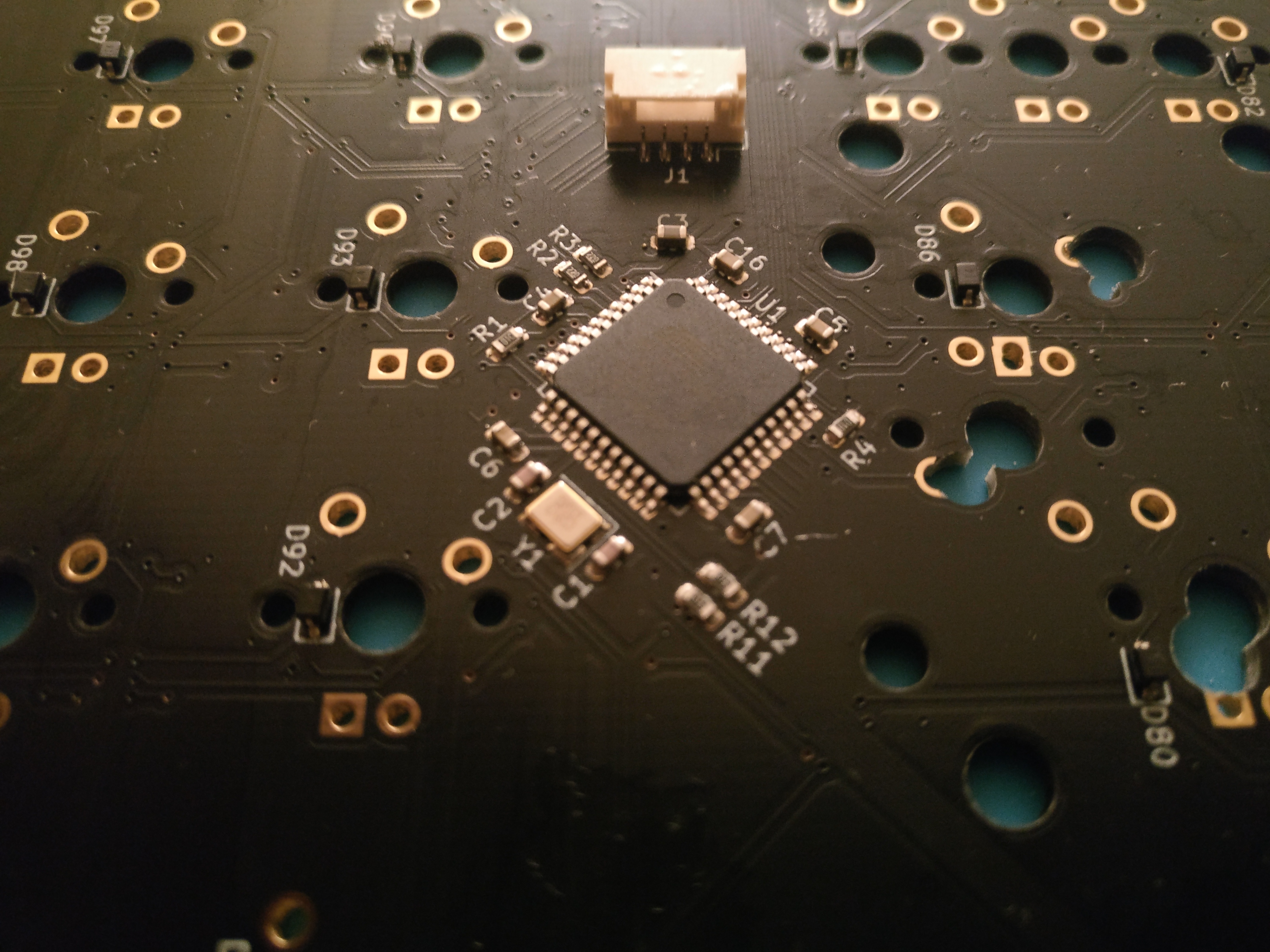
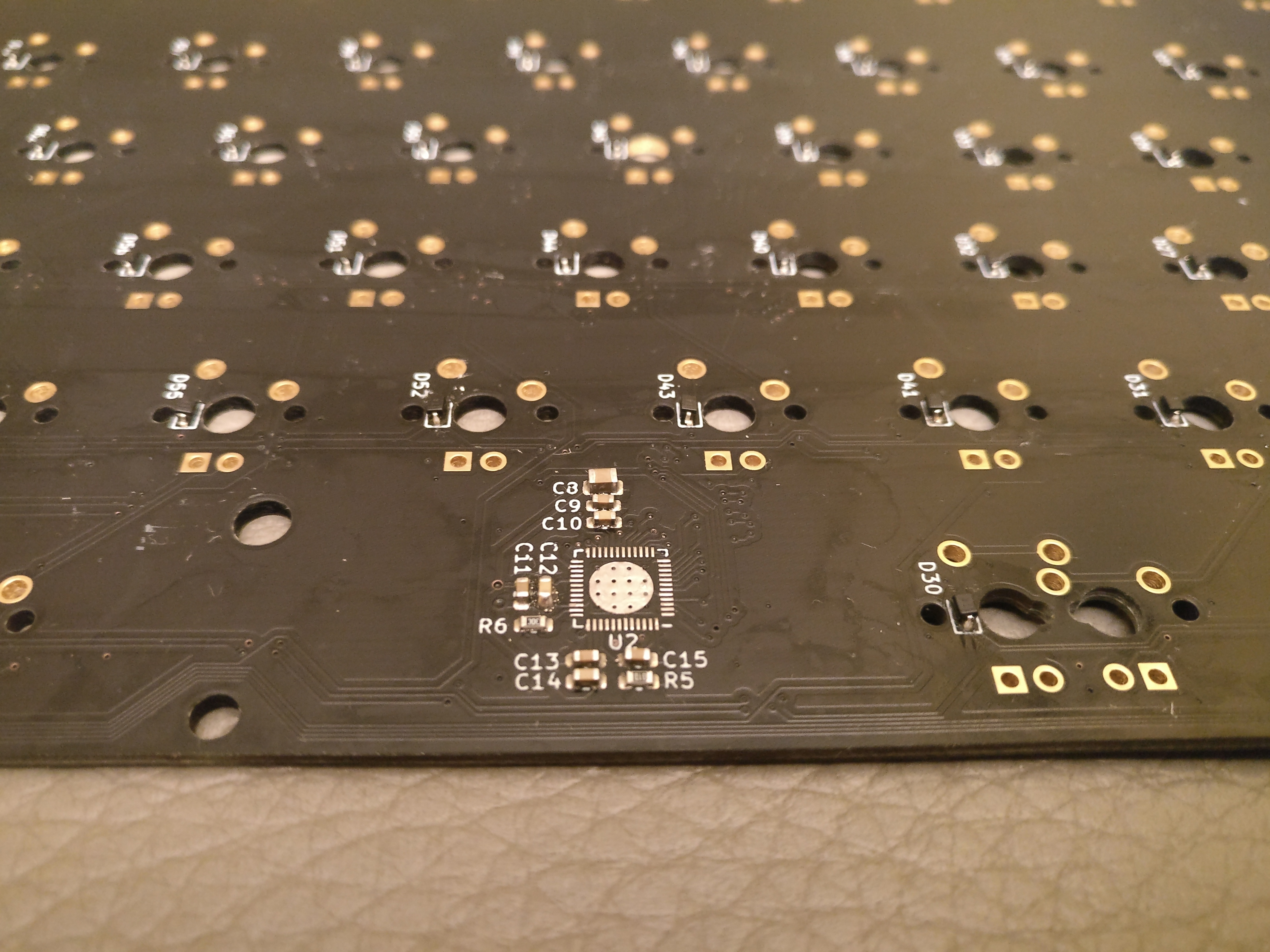
The PCB(s):

  • No more hotswap sockets, simple soldered switches with plate and pcb mount compatibility.
  • Goodbye Costar stabs, Cherry PCB mount stabs used instead.
  • Increased layout customization, welcome to the PCB Swiss Cheese effect :wink:
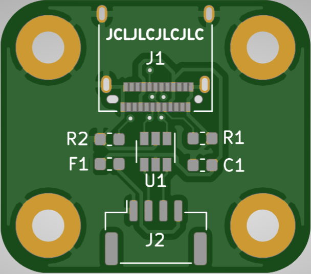
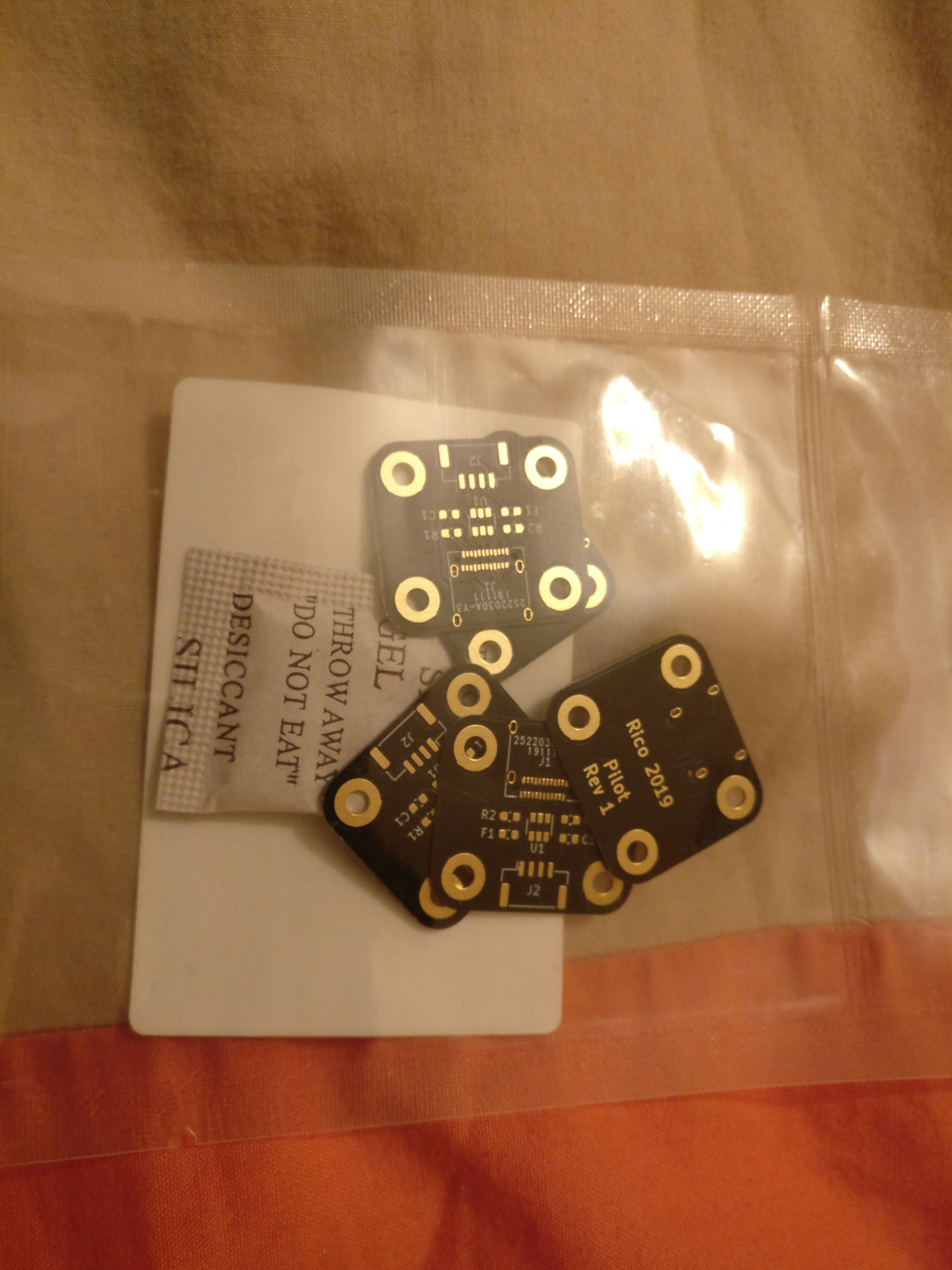
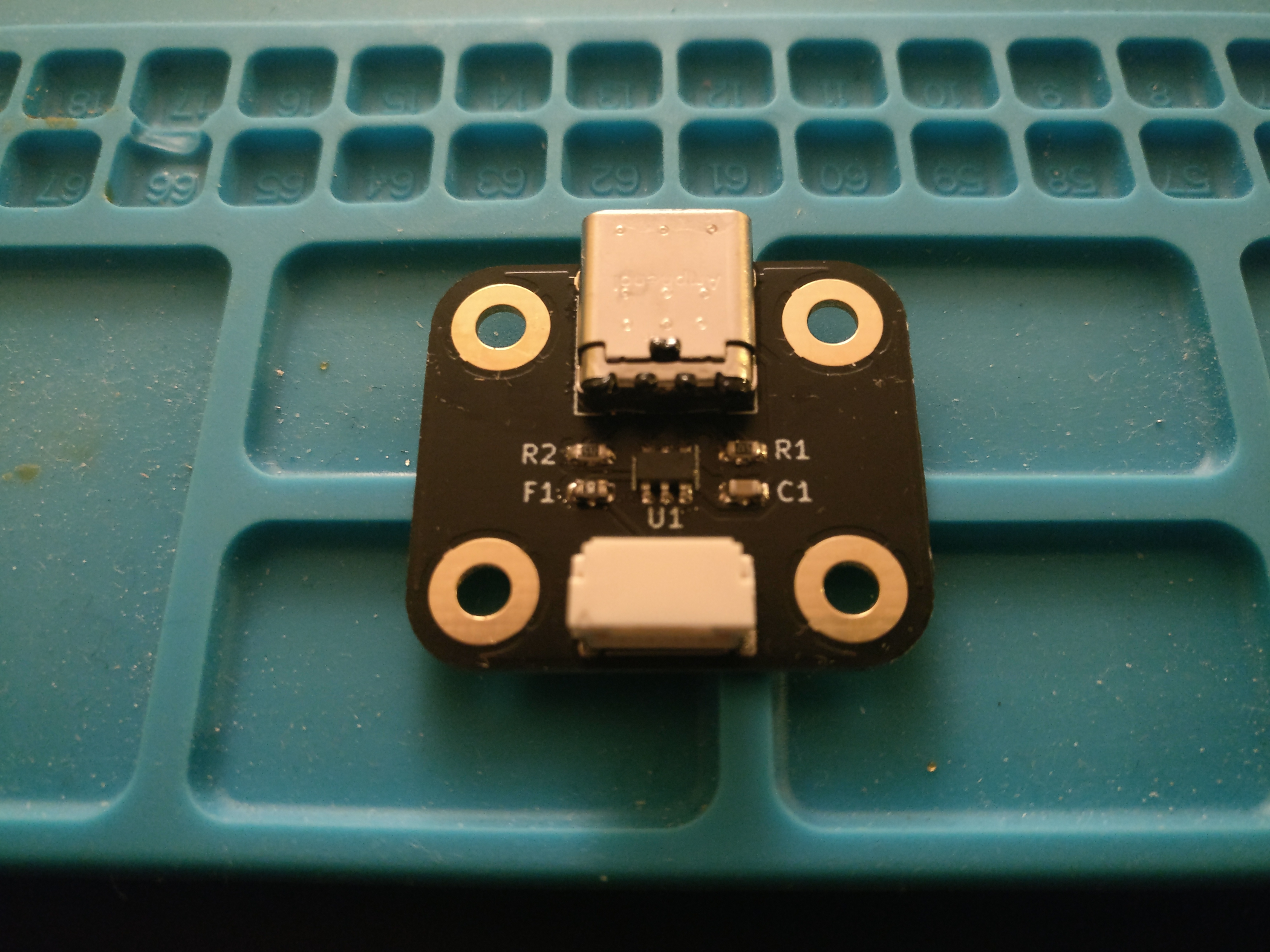
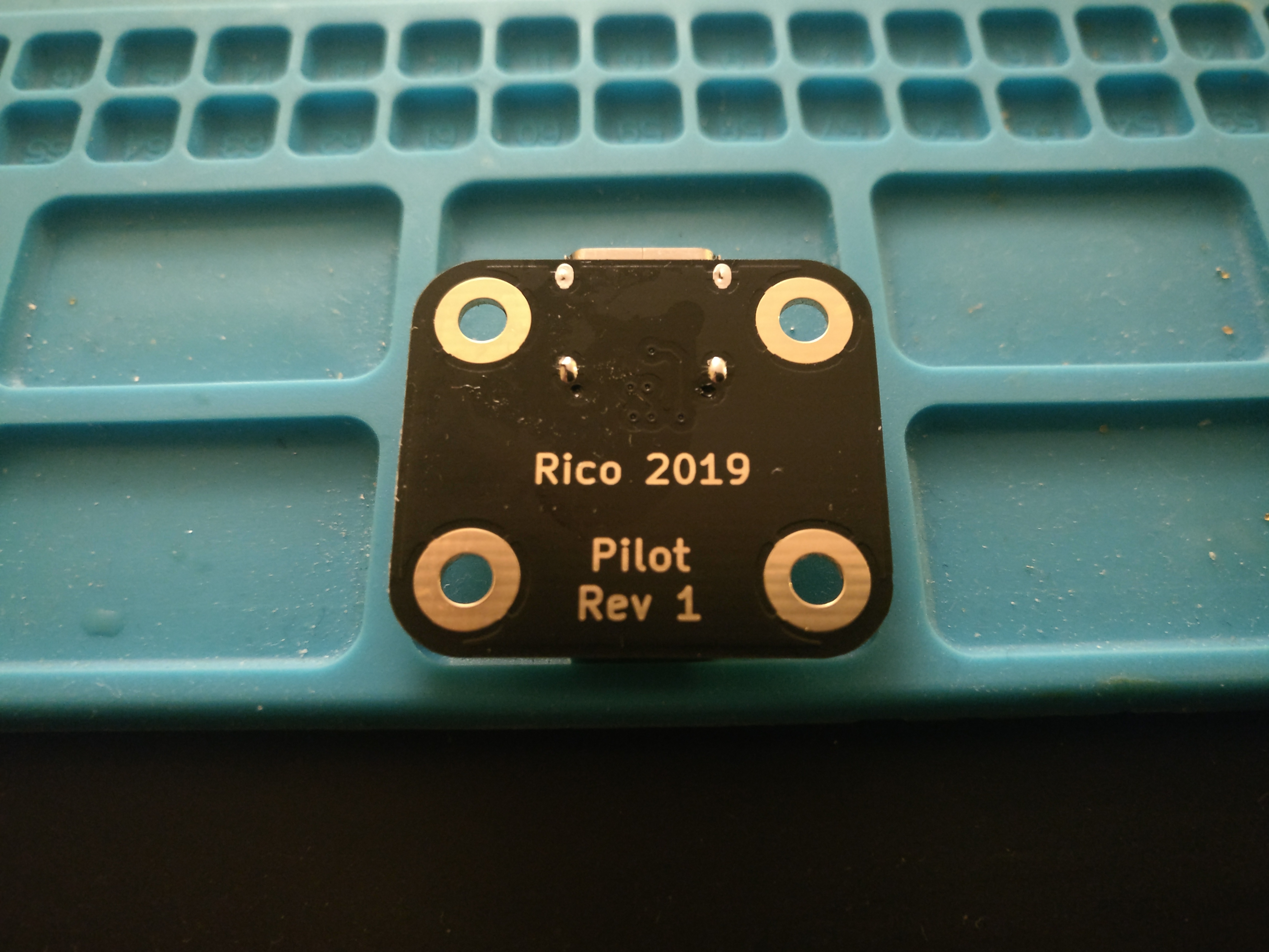
  • Separate daugther board PCB with USB C, ESD and over current protection.
  • No capslock/numlock/scrolllock led indicators to keep case design uncluttered.
  • In-switch monochrome LED lighting, independently adressable.
  • ATMEGA32U4 MCU:
    • Try to do more stuff with less available pins than the previous project that used an AT90USB1286 MCU.
    • It is a funny personal challenge.
    • Smaller package makes it easier to find a place in the PCB.
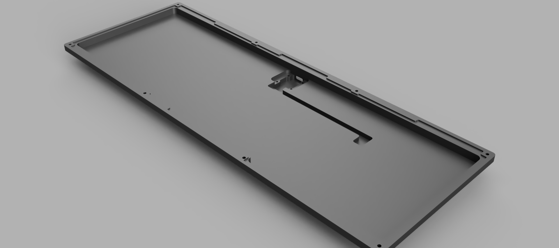
The case:

  • Two parts design.
  • All anodized aluminium.
  • No integrated plate.
  • So no brass or steel weights and no complicated design in order to lower price.
  • Probably sandwitch plate design:
    • I’d love to take inspiration from @Wilba’s work on spring plate design for it’s Thermal.
    • Absolutely genious idea that he had, just watch @TaehaTypes build video and you will understand.

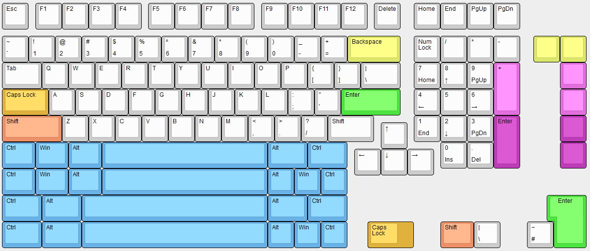
This will be a 1800 layout with the following compatibility:

Progress done:

  • PCB design well advanced, now tuning and double/triple/quadruple checking it.
  • Draft case design, may change depending on plate design choice.

See you soon!

9 Likes

I was wondering whether you might be inspired to have another go…very much looking forward to following along!

1 Like

Hello @jshufelt!

I was wondering that also … and needed a bit of rest :stuck_out_tongue:
But, oh my oh my, here we go again for struggling times :smiley:

PS:
I’m eagerly waiting for your next build log :slight_smile:

1 Like

Hey,

Here are some news on the project.

I’ve carefully checked the PCBs several times and they look ok.
So here are some renders below, using tracespace.io website(https://tracespace.io).

The main PCB:

The USB daughter board:

One of the goals in the making of this keyboard is to learn new things.
This is why I wanted to experiment designing a keyboard with individually addressable leds and some flexibility for the keys layout.

As for the layout flexibility, this has turned into numerous DRC errors in Kicad because of pads and holes intersecting each other.
I tried to resolve them and asked questions to other makers in this forum, and came to the conclusion not to try to remove them:

  • This is what we commonly see in these swiss cheese PCBs.
  • These will not prevent PCB to be manufactured anyway.
  • These errors were always listed first in Kicad DRC report and with specific message so could be easily ignored wihout forgetting the other important errors that were coming.

This time I used ai03 Cherry MX schematics and footprints.
The footprints in particuliar are very well made:

  • They have a drawn white bounding box that is exactly at key intervals.
  • So exactly 19.05 x 19.05 mm for a 1U unit for example.

This make switches placement on the PCB a breeze: you just have to ensure that neighbouring keys have coincident edges.
Here is the download link of these for people that are interested:

You may have seen the string “JLCJLCJLCJLC” on the silkscreen part of the PCBs.
As I plan to use JLCPCB services for at least the main PCB this is a little trick to place their serial number were we want on the PCB.
For people that use this PCB manufacturer here is the link that explain more in detail how to proceed:

I wanted not having to solder 100x small SOD323 diodes, plus the CPU, resistors and capacitors by hand:

  • Takes too much time.
  • This is error prone.
  • Learned that by screwing 3 PCBs before having a working one last time :smiley:

So I plan to use JLCPCB new PCBA service, at least for the main board.
They have some limitations:

  • Only green soldermask.
  • Soldering on one side only(not a problem).
  • Don’t have all the components needed.

Anyway I should be able to have everything soldered but the led driver and the JST GH connector, good :stuck_out_tongue:
I will need to learn how to generate and provide a suitable file for the manufacturer pick and place machine: Kicad seems to do at least half of the job with their .pos file format.

I also looked for PCB manufacturer alternatives that are not in China and still have decent pricing.
I came by the name of Aisler:

  • PCB manufacturing done in Germany.
  • They seem to recently provide PCB manufacturing in the USA as well.
  • Not crazy expensive, and shipping is free.
  • They can also provide you electronic components and stencil if you want.
  • Only green soldermask and ENIG finish.

I was curious and ordered 3 USB daughterboard PCBs and a stencil, we’ll see how they come soon.

3 Likes

I tried to use JLCPCB PCBA service but had problems using it.
I had a few back and forth email exchange with the support (very reactive) and came to a BOM and CPL file that was kind of working.
But in the 3D preview some components were no visible and others not at the right position.
It looks like other people have had similar problems, the preview window is still unstable and they seem to work hard to make it better.
Keep in mind that this service is very new and will work better as time goes on.
As I don’t want to order without being sure that all components are well placed I will abandon using this service for this project. Maybe for the next one it will work ok ?

Still I ordered PCBs from them as their quality is good and the price very low.
The Pilot and Winghead PCBs have been validated for manufacture, now is the time to wait for hem to arrive.
They are all black(mate?) soldermask with ENIG finish, standard 1.6mm thickness for the Windhead and 0.8mm for the pilot(to accomodate the USB C connector that has very short 1mm through hole mount tabs).

Also ordered most of the components at their sister company LCSC as their price is incredibly low for all passive components: for the diodes alone it was more than 20$ cheaper than standard suppliers!

I received Pilot PCBs and stencil from Aisler and was satisfied by the general quality.
I ordered the stencil for the Wingead PCB at their house and I will definitely use their service in the future for smaller prototyping boards.

2 Likes

Just received my PCBs!
These are looking good and I like the black satin solder mask finish on them.
Also all components have been received.
Now need spare time to solder one and see if it works.

Waiting for these I started designing the case on Fusion360, it starts to take shape :wink:

8 Likes

I had a bit of free time today, so decided to solder the USB daughterboard.
It was also the time to test how good was the new solder paste I recently purchased.
I’m exclusively using lead free solder but was disappointed by the previous solder paste I had, too consistent and had to really heat the board to melt it, it was not the case of the first ever one I bought a long time ago.

For the standard unleaded solder paster you have to push well over 220°C to be able to melt them.
The one I purchased is a bit special: it is a low temperature solder paste and melts at only 185°C.
They do that by adding bismuth to the metal alloy.
There seem to have some caveats:

  • Lower mechanical properties of the solder joints, adding silver seems to alleviate that(there is 0.4% silver on mine, can go up to 1%).
  • If you put leaded solder in contact with the solder joints, they will melt later on at a temperature of only 95°C.

It comes with 2 plastic compartments with solder balls on one side and flux on the other, just have to push flux compartment into the solder balls one and mix. Voila!

I had ordered a stainless steel stencil at Aisler for dispensing the solder paste.

Now time to put solder paste and see how good it is, my cheepo hot air station configured at 220°.


Sorry for my really dirty silicone mat…

Well this is fantastic, no problem melting every solder joints, including the ones of the USB connector.
I’m happy of the consistency of this solder paste, and not having to heat components like crazy is a big plus!

These PCBs are only 0.8mm thick and you can see that the USB chassis pins are barely protruding on the other side, it has been a bit tricky to hand solder then later.
Once cleaned with isopropyl alcohool and all micro solder balls removed(you can see some in this image if you are carefull) it is good to go!

Next time will be the turn of the big boy, but no free time for this year unfortunately :frowning:

4 Likes

I have been quite busy these last weeks, no time to solder the main board PCB … but could still work on the case design bit by bit :wink:
So here are some renders(very bad, just figured out how to do that quickly today on Fusion 360).

The design should not change by much, still have to work on case dimension tolerances in order for the top part to slide on the bottom part; this will depend on the type of finish I’ll want (anodized of powder coat) and the machining precision (will depend somehow on the manufacturer and price).
I made sure that everything fits nicely together in order to avoid really stupid mistakes, that is position every parts on Fusion360 including the PCBs.
The test fit is done by doing several section analysis views, like the one below.

As you can see there is no much place left between the PCB and the bottom case, there is only 2 to 3 millimeters of space.
To ensure that the PCB is not making contact with the case, the plate can flex down by 1 millimeter maximum before hitting the bottom case.
This technique is very similar to the one done by @Wilba on it’s Thermal case design.
Speaking of him, I told you before that I found his leaf spring plate design an ingenious idea so I tried to replicate it my own way, taking care of not doing a rip-off.
So here is a view of the plate alone to give an idea of what I’ve come with.

You may see similarities with Wilba’s Thermal design:

But there is also similarities with new leaf spring plate design of the Keycult n°2:

I figured out these similarities after having mostly finished my own design, let’s hope it means I did it right :stuck_out_tongue:

There is a 1mm cutout on the bottom case for the plate to flex for that amount, and the same shaped cutout on the top case, but of only 0.5mm, for the plate to spring back without hitting the top case.
The (horrendous) render of the bottom case below give an idea of were and how the cutouts are made.

Now need to take time to solder this main PCB and ensure that it works before paying big money to manufacture the case.

6 Likes

I really like where this is heading :eyes:

2 Likes

Looking good!
Just a question, why not mount the daughterboard parallel to the table?
Okay, another question. How thick are the walls on the bottom? 2mm?

I just might copy your switch plate design. :grin:

Looking forward to updates!

1 Like

I am liking that side profile.

1 Like

Just a question, why not mount the daughterboard parallel to the table?

Good question :wink:
I wanted to make the CNC manufacturing easy, with the less setups possibles on a 3 axis machine.
Having the daugherboard parallel with the top section makes it possible to machine the motherboard cutout on the same setup for the top part, so the part could theorically be done with only 3 setups on a 3 axis machine:

  • top part with daugherboard cutout.
  • backside part for USB cutout.
  • bottom part.

If I had made the daughterboard parallel to the table it would add at least one setup stage to compensate for the 5 degree slope of the case on a 3 axis machine.
On a 4 axis machine this should not add any setup stage as you can rotate the piece during machining, but I don’t know in advance what the manufacturer will use so I played safe to reduce the costs :stuck_out_tongue:

Okay, another question. How thick are the walls on the bottom? 2mm?

Yes, it is 2 mm.

I just might copy your switch plate design.

Feel free to do it!
Although I don’t know yet how it will perform in real life.

I wanted to make the CNC manufacturing easy, with the less setups possibles on a 3 axis machine.

I didn’t think of this. I might change mine as well.

Yes, it is 2 mm.

And here I am, limiting my designs to 3mm

Feel free to do it!
Although I don’t know yet how it will perform in real life.

Thanks!

A little bit of news.

Still had no time to solder the main board as I need half a day to do that(I like to take my time to reduce chances of mistakes).

But I could polish the case design further:

  • Add tolerances here and there.
  • Increase some wall thickness.
  • Add bumpon cutouts.
  • double/triple/quadruple check that everything fits as intended(and fix some errors by doing that).

Being more confident of the design I ordered plates at LaserBoost.
See this beautiful sandblasted brass piece in the picture below :stuck_out_tongue:

And ordered switches, leds, and screws…

Looked at possible manufacturers for the CNC job, preferably in Europe to favour one of my neighbouring countries. This part also progressed quite well recently.

3 Likes

That plate looks so fun! It reminds me of t0mb3rry’s flex plate he made for his CA66:

It’s kinda like it’s own pseudo leaf spring in a way. I do wonder if a lot of the flex will be loss on yours going with brass though since it can be so stiff :thinking:

Regardless, it looks beautiful :slight_smile: I can’t wait to hear it sing!

2 Likes

Oh, very interesting plate design!
Yes it is quite close on the principle.

Having the plate in brass will be obviously stiffer than say aluminum or FR4.
But the leaves are quite thin, 2mm, so it remains to be tested to judge.
The design was done to accomodate different materials, and FR4 is another one I was interested on.
I may later on send it to a PCB manufacturer, I’m very curious to see the resulting flex and sound.

I had at last one full afternoon yesterday to solder the big boi :slight_smile:
This was with a lot of excitement and stress that I started this endeavour.
SPOILER: lots of potato pics will follow :sweat_smile:

First things first, time to organize myself and most of all the SMD components that I will soon solder on the board.
Found a great idea on the net some time ago, that is stick all components with double side tape on a cardboard and write component labels on it with orientations if needed.
This resulted in something like this:

Then onto placing the stencil on the PCB. Last time I had solder paste consistency problems because the stencil was not firmly seated on the PCB and could move up a bit, this can result into solder bridges and residual solder balls.
So I surrounded the PCB to solder with other PCBs I had and put a lot of tape all around, this stencil will not wiggle anymore.

Now time to put my trusty low temp solder paste onto the PCB, the result is much better than before with pads clearly defined and no residual solder paste everywere.

As for the LED driver the pitch of the pads are so fine that I couldn’t manage to see if the stencil was correctly aligned enough (my old eyes can’t keep up anymore), so decided not to spead solder paste on it, only on the components that surrounds it.

Onto placing components on the PCB.
Using sweezers for a few ICs, capacitors and resistors is ok but one hundred diodes is not, so looked again on the net for some alternatives, pick and place pens.
The ones you find are cheap but useless piece of crap … until you modify them a bit :wink:
I ordered an aquarium pump, modify it to reverse the air direction (to suck air instead of pulling it) and pimped the useless pen to make something useful out of it. A little bit of tubing and voila !

This proved to be much more efficient than using tweezers with a bit of practice. Could be improved as for the moment I have to fill a hole on the pen with my finger, maybe have a foot switch pedal would be more convenient.

A good pass of my cheapo hot air station and this was quickly soldered.
… But some diodes could not stay in place due to some slight misalignement issue and because there is so little solder paste on these SOD323 pads. Finished the job using my iron worstation, this took quite a while :frowning:
SOD323 footprints are a b**ch to solder, I may look for 603 versions for a next design.

The result is quite nice with a even amount of solder on the pads and no/few solder balls.

I tried to solder the LED driver on the last stage but this damn thing didn’t want to align itself on the pads with the surface tension of the solder, sliding out of it’s place and about to touch the surrounding components. I finally gave up after the third try and cleaned the pads, this PCB will be without lighting (not that I care that much of being bling bling :stuck_out_tongue: ).

Before plugging that onto my PC and frying another USB port on it :rofl: 
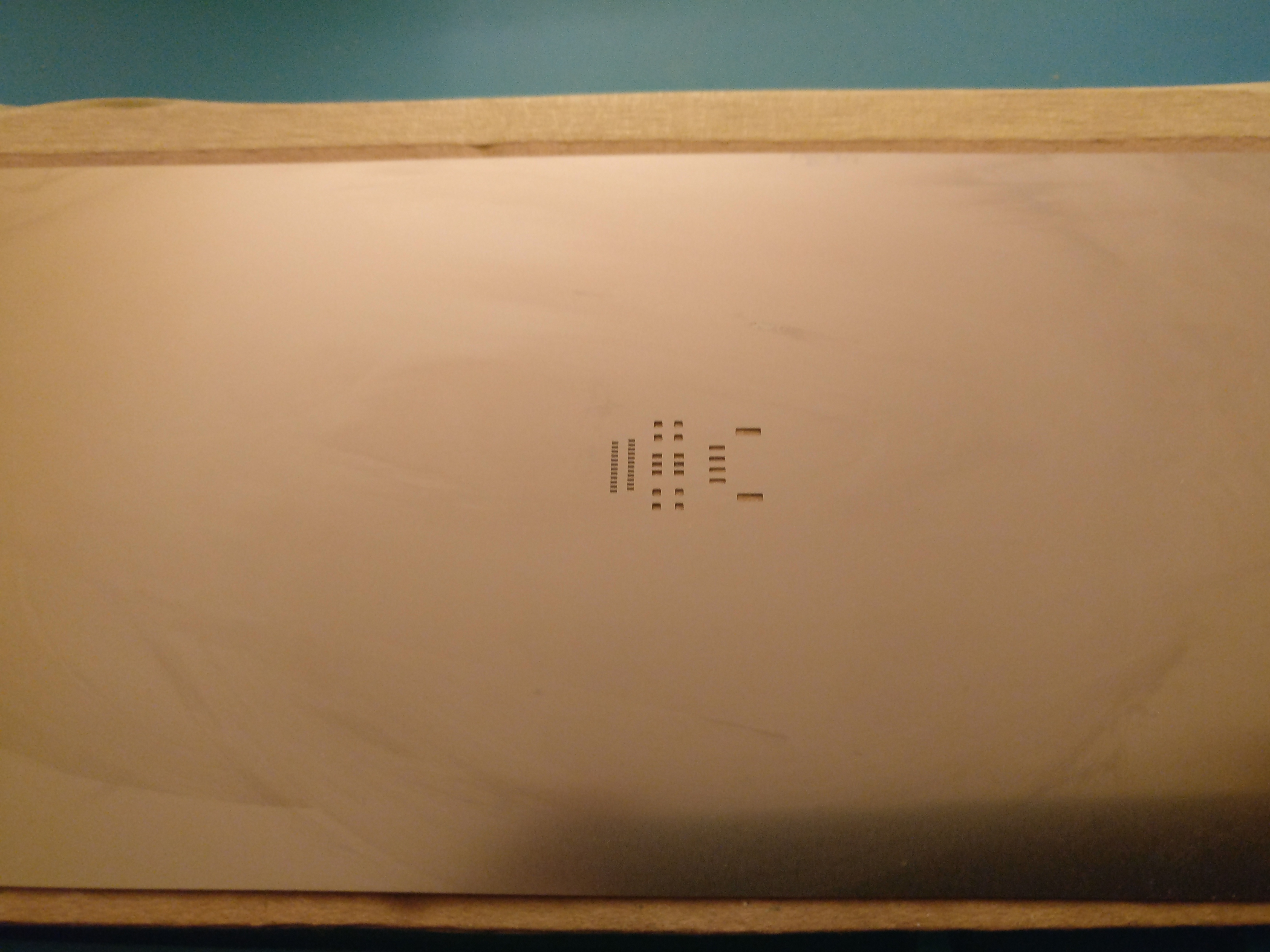
I did some basic tests with my multimeter, like:

  • No 5v to GND short.
  • USB signal D+/D- goes correctly from the daughter board to the main board.

Good to go, time to plug this thing and see what happens …

Nothing … after the third desperate plug/unplug attempt (the time for Windows to find the drivers :rage: 
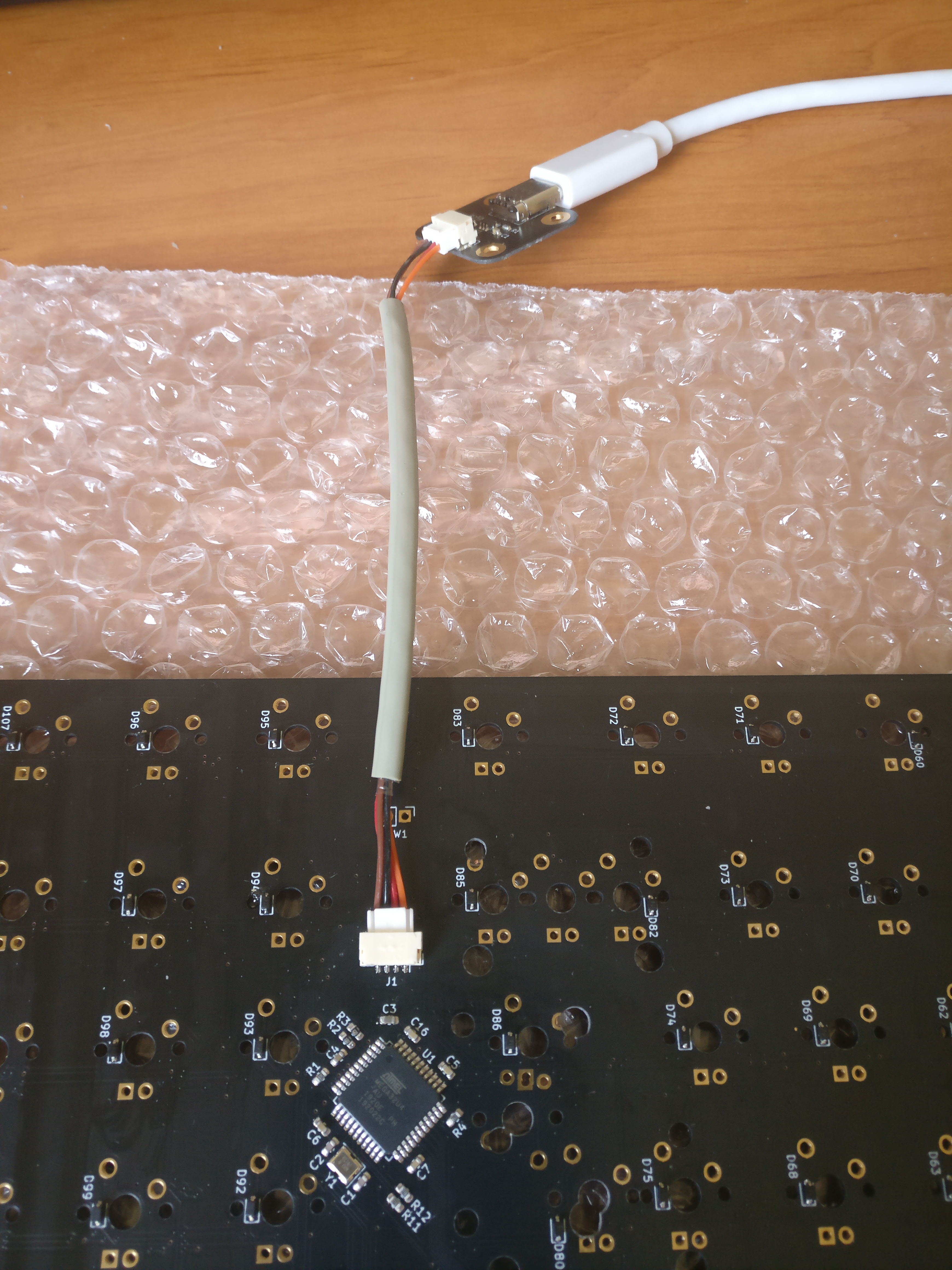
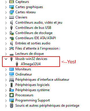
) I had this nice view on my device window :partying_face:

Hes_Alive

Hurray!
I still don’t know if the switch matrix will have any errors ( I need to do some QMK programming for that ) but at least USB communication and MCU are working :smiley:

6 Likes

I love all of the detail here - between this log and your Simply96 project, it’s great to see all the steps from concept through execution to completion. In this case, it’s great to see how you go about SMD soldering. That’s a bridge I have yet to cross…

1 Like

Thank you!

The amount of equipment needed is not that crazy and you can do with less.
I remember my first PCB with SMD components (it was custom designed ecig DC/DC controller), all I had was my kitchen hot plates and an IR thermometer to guess the soldering temperature :smiley:

1 Like

Great post, thanks for sharing! I always have trouble with my stencil sliding when I’m applying solder paste. I’ve been using framed stencils, but now I wonder if I should get one without a frame and just tape it in place like you’ve done here…

Also, good tip about pick and place pens! I’m going to look into them.

1 Like